多層電路板的芯板工藝特性
1 Overview
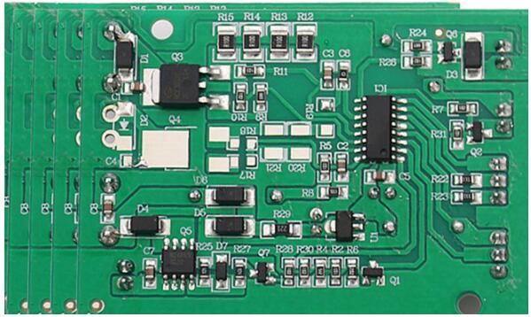
is currently designed by a complex circuit, 而將這種複雜的電路設計成薄而輕的覈心板離不開 多層電路板(MLB) manufacturing 科技.
多層電路板(MLB) 製造技術 has developed rapidly, 尤其是在2.0世紀8.0年代末. 隨著高密度I數量的新增/O (input/output) leads, 超大規模集成電路的產生與發展, ULSI集成電路, 和SMD設備, SMT採用 多層板 促進了多層板的製造技術達到了非常高的工藝水準. 作為“光”, 薄的, 短的, “小”部件被廣泛使用, SMD的快速發展與SMT的普及, 互聯科技變得更加複雜, 以及 多層板 提升為細線寬和窄線寬. 拋, 更瘦更高, 微孔徑的發展. 的轉變 多層印刷電路板 technology, 那就是, 多層印刷電路板 manufacturing technology, 已廣泛應用於民用電器.
MLB的開發通常根據應用範圍分為兩類:一類是用作電子整機的基本部件, 用於安裝電子元件和互連基板; 另一種用於各種類型的晶片和集成電路晶片的載體板. 用作載體板的MLB導電圖案更加精細, 基板的效能要求更加嚴格, 制造技術更複雜.

2. 工藝特點 多層印刷電路板 are as follows:
1., High density
The high density of multi-layer circuit boards means that the use of high-precision wire technology, 微孔徑科技, 而窄環寬或無環寬科技大大提高了印製板的組裝密度. The basic status of multi-layer circuit board high-density interconnection technology is shown in the following table (Table 2-1):
2., high-precision wire technology
High-density interconnect structure of multi-layer circuit boards, 所使用的電路陣列需要線寬和間距為0的高精度導線.05-0.15毫米. 相應的制造技術和設備必須具備形成高精度的科技和加工能力, 高密度細線.
3., Micro-aperture technology
With the shrinking of the aperture of the 多層電路板, 對鑽井工藝和設備提出了更高的科技要求. 同時, 要解决小孔鍍層的附著力和延展性問題,必須採用全化學鍍和直接鍍科技.
4., the ring width of the reduced hole of the core board
The reduction of the ring width around the empty space can increase the wiring space, 從而進一步提高 多層電路板.
5., multi-layer circuit board structure diversification
With the high stability and high reliability requirements of precision devices, 密度要求 多層電路板 製造業以及互連數量和複雜性的新增, 其結構的多樣化是不可避免的.
6., Thin and multilayer technology
Thin and multilayer technology is fully adapted to the technical requirements of "light, 薄的, 短的, “小”和高密度組件. 當前制造技術科技的發展趨勢 多層電路板s分為:高級薄板和普通薄板. 高層建築的厚度 多層電路板 將為0.6-5.0毫米, 層數為12-50層或更高; 薄的厚度 多層電路板 將為0.3-1.2毫米, 層數為4-10層或更高.
7., 埋葬的, blind and through-hole combined multilayer board manufacturing technology
This type of 多層印刷電路板 具有複雜的結構,將通過大量的電力互連科技來解决, 可將佈線密度提高50%,並大大降低生產細線和小孔徑環寬的壓力.
8., 多層佈線 多層電路板
多層佈線的結構 多層電路板 在無銅基板表面塗有粘合劑, 然後利用電腦提供的數據控制配線機, 和0.06-0.1MM方形漆包線在X和Y方向上相互垂直. 裝電線, 然後在45°對角佈線, 鋪設在基板兩側. 接線完成後, 用薄膜覆蓋,起到固定和保護作用. 它是固化和數控鑽孔等工藝.
9., direct writing technology
Using direct writing technology can completely and quickly produce prototypes (that is, 自由成形3維製造, 雷射燒結, 金屬印刷科技, 等.) to produce prototypes with three-dimensional structures and characteristics.
直接書寫的優點是它的範圍相對較廣,可以對電子系統的製造產生影響.
iPCB是一家專注於開發和生產高精度PCB的高科技製造企業. iPCB很高興成為您的業務合作夥伴. 我們的業務目標是成為最專業的原型 PCB製造商 在世界上. 主要專注於微波高頻PCB, 高頻混合壓力, 超高多層集成電路測試, from 1+ to 6+ HDI, Anylayer HDI, IC基板, IC測試板, 剛柔PCB, 普通多層FR4 PCB, 等. 產品廣泛應用於工業4.0, 通信, 工業控制, 數位的, 權力, 電腦, 汽車, 醫學的, 航空航太, 儀器儀錶, 物聯網及其他領域.