PCB戰鬥技能
在開始新的設計時,由於大部分時間都花在電路設計和元件選擇上,在PCB佈局階段,往往經驗不足,考慮不足。
如果沒有提供足够的時間和精力來設計 PCB佈局 階段, 當設計從數位領域轉換到物理現實時,可能會導致製造階段的問題或功能缺陷.
那麼,設計一個 電路板 這在紙上和實物上都是真實可靠的? 讓我們探索前6名 PCB設計 設計可製造產品時需要瞭解的準則, 可靠的PCB.
01. Fine-tune your component layout
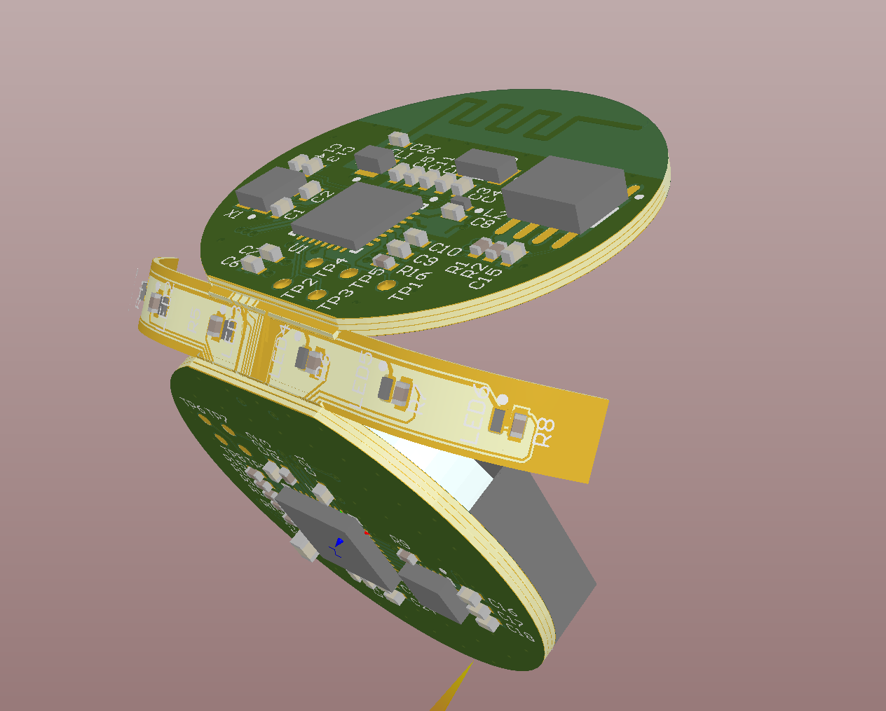
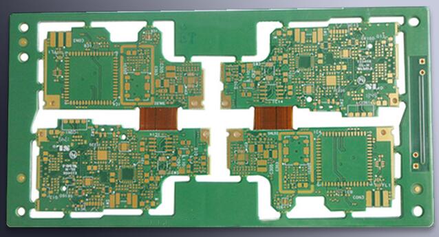
The component placement stage of the PCB佈局 過程既是科學也是藝術, 需要對上可用的主要組件進行戰畧考慮 電路板. 儘管這一過程可能具有挑戰性, 您放置電子元件的管道將决定您的 電路板 是製造和如何滿足您的原始設計要求.
儘管有組件放置的一般順序, 例如放置連接器, 印刷的 電路板 安裝裝置, 電源電路, 精密電路, 和關鍵電路, 要記住一些具體的指導原則, including:
Orientation-Ensure that similar components are positioned in the same direction, 這將有助於實現高效且無錯誤的焊接過程.
佈置避免將較小的組件放置在較大的組件後面, 囙此,小部件可能會受到大部件焊接的影響,並導致安裝問題.
Organization-It is recommended to place all surface mount (SMT) components on the same side of the 電路板, and place all through-hole (TH) components on the top of the 電路板 最小化裝配步驟.

一場決賽 PCB設計 需要注意的準則是, when using mixed technology components (through-hole and surface mount components), 製造商可能需要額外的過程來組裝 電路板, 這將新增您的總體成本.
Good chip component orientation (left) and bad chip component orientation (right)
Good component placement (left) and poor component placement (right)
02. 正確放置電源, 地 and signal wiring
After placing the components, 你可以放置電源, ground, 和訊號跟踪,以確保您的訊號有一個乾淨和無故障的路徑. 在佈局過程的這個階段, keep in mind the following guidelines:
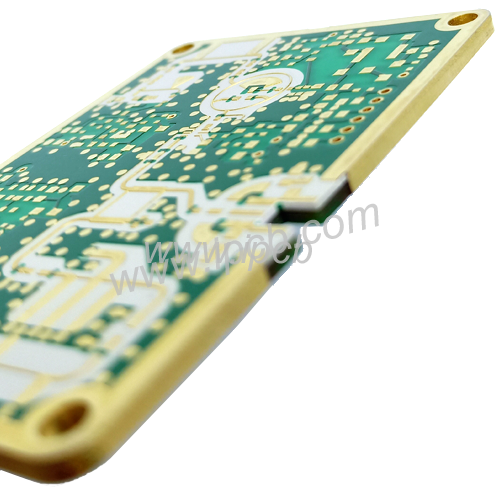
1) Locate the power and ground plane layers
It is always recommended to place the power and ground plane layers inside the 電路板 同時保持對稱和居中. 這有助於防止 電路板 從彎曲, 這也與組件的正確定位有關.
用於為IC供電, 建議為每個電源使用公共通道,以確保堅固穩定的軌跡寬度, 並避免組件之間的菊花鏈電源連接.
2) Signal wire routing connection
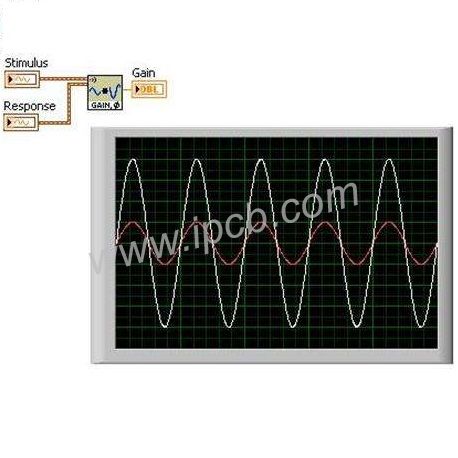
Next, 根據示意圖中的設計連接訊號線. 建議始終採用最短的可能路徑和組件之間的直接路徑.
如果您的組件需要固定並在水准方向上放置,且沒有偏差, 建議將導線基本水准敷設在 電路板 外出交際, 然後在佈線後穿過垂直佈線.
以這種管道, 隨著焊接過程中焊料的遷移, 組件將在水准方向上固定. 如下圖上部所示. 下圖下半部分的訊號佈線方法可能會在焊接過程中焊料流動時導致組件偏轉.