印刷的 電路板 production process
1. Process flow of single-sided printed board:
Blanking - Screening Missing - Corrosion - Removal of Printing Material - Hole Processing - Printing Mark - Applying Flux - Finished Product.
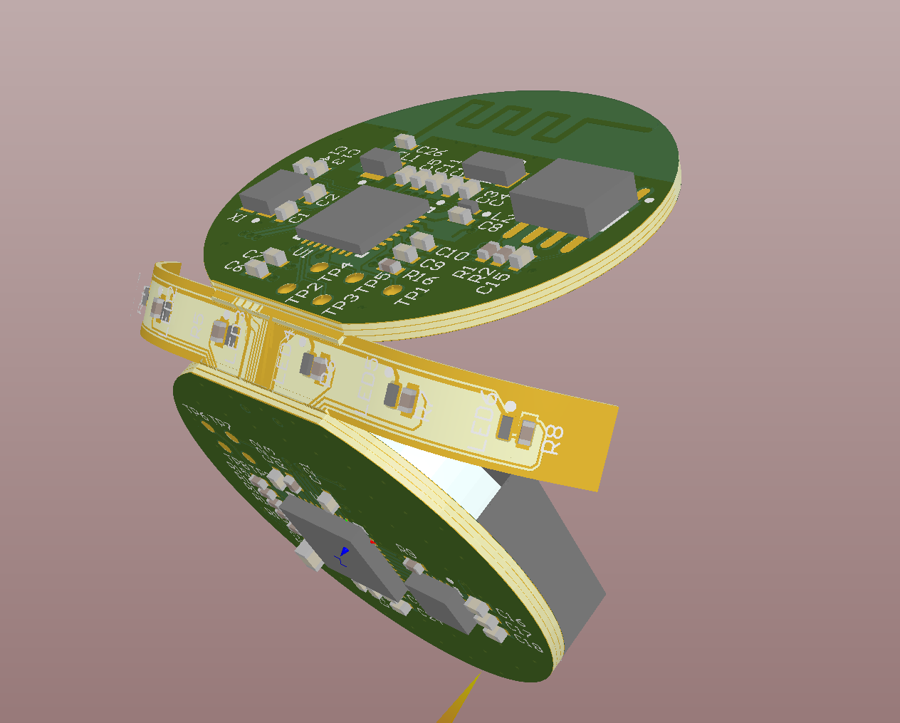
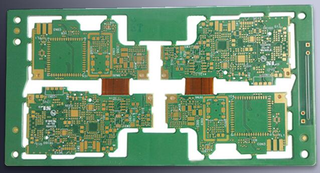
2 Process flow of 多層 printed board:
Inner layer 材料 processing - positioning hole processing - surface cleaning treatment - inner layer wiring and graphics - corrosion - pre-laminating treatment - outer and inner layer 材料 lamination - hole processing - hole metalization - refers to outer layer graphics - plating corrosion resistance Weldable metal-Removal of sense-Light glue corrosion-Plug gold plating-Shape processing-Hot melt-Flux application-finished product.
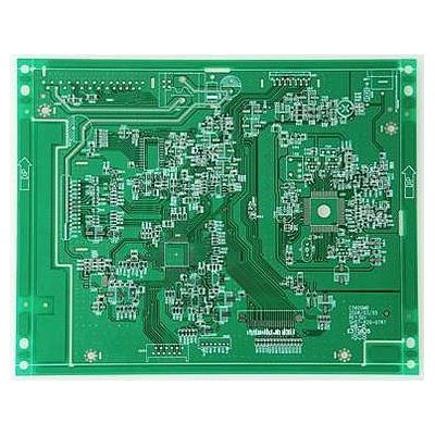
The function of the printed circuit board

The printed 電路板has the following functions in electronic equipment:
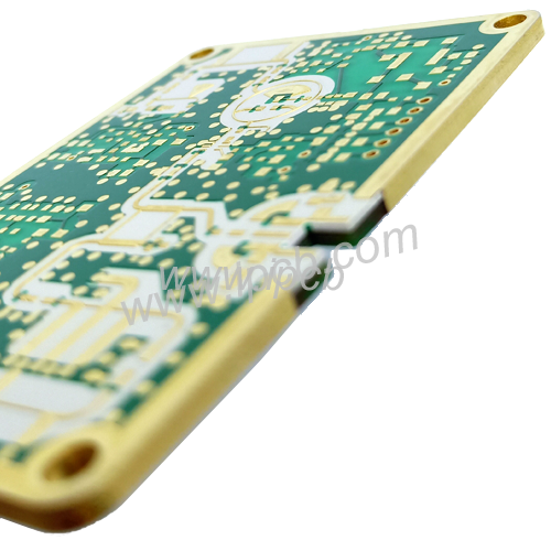
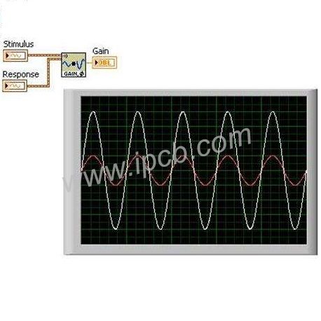
Provide mechanical support for the fixing and assembly of various electronic components such as integrated circuits, 實現集成電路等各種電子元件之間的佈線和電力連接或電力絕緣, 並提供所需的電力特性.
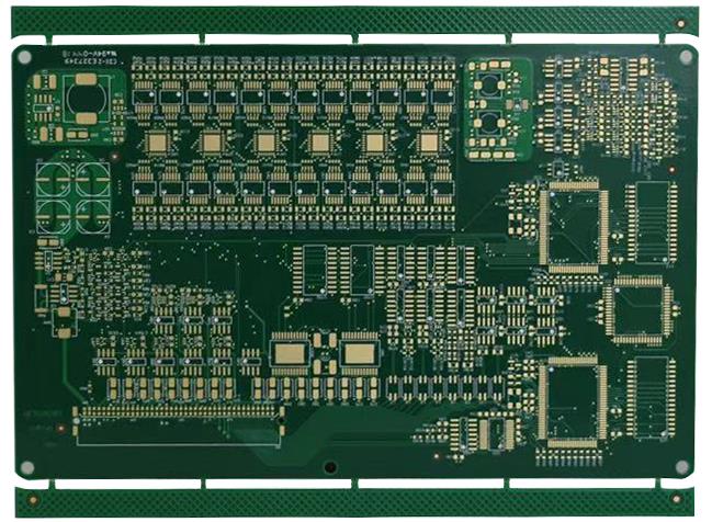
為自動焊接提供阻焊板圖形, 並為元件插入提供識別字元和圖形, 視察, 和維護.
電子設備採用印製板後, 由於類似印製板的一致性, 可以避免手動接線錯誤, 電子元件可以自動插入或安裝, 自動焊接, 和自動檢測, 確保電子產品的質量. 提高勞動生產率, 降低成本, 便於維護.
The development trend of printed circuit boards
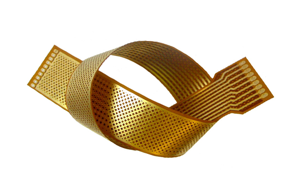
Printed boards have developed from single-layer to double-sided boards, 多層板和柔性板, 繼續向高精度方向發展, 高密度、高可靠性. 不斷縮小的體積, 降低成本, 效能的提高使印製板在未來電子產品的發展中保持了强大的生命力.
未來印製板製造技術的發展趨勢是向高密度方向發展, 高精度, 細孔徑, 細金屬絲, 小間距, 高可靠性, multilayer, 高速傳輸, 重量輕, 效能更薄.
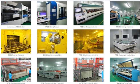
iPCB很高興成為您的業務合作夥伴. 我們的業務目標是成為最專業的原型 PCB製造商 在世界上. 在這一領域有十多年的經驗, 我們致力於滿足不同行業客戶的質量需求, 傳送, 成本效益和任何其他苛刻要求. 作為最有經驗的人之一 PCB製造商中國的s和SMT組裝商, 我們很自豪能成為您最好的業務合作夥伴和PCB需求各方面的好朋友. 我們努力使您的研發工作輕鬆無憂.