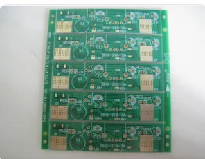
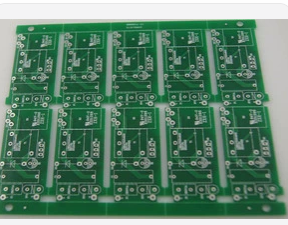
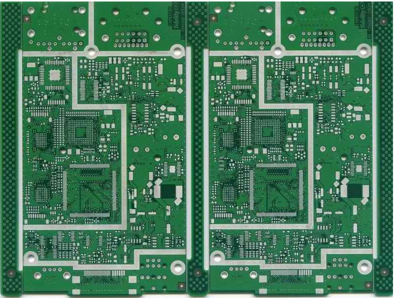
中的十個常見問題 PCB設計
1 Overl一p of pads
1. The overlap of the pads (except the surface mount pads) means the overlap of the holes. 鑽井過程中, 由於在一個地方多次鑽孔,鑽頭會斷裂, 導致孔損壞.
2、多層板上有兩個孔重疊。 例如,一個孔是隔離板,另一個孔是連接板(花墊),囙此薄膜在拉伸後會顯示為隔離板,導致報廢。
第二,濫用圖形層
在一些圖形層上進行了一些無用的連接. 原來是 四層板 但設計了五層以上的電路, 導致了誤解.
2. 它在設計圖形時省去了麻煩. 以Protel軟件為例,用Board層繪製各層的線條, 並使用線路板層標記線路. 以這種管道, 執行燈光繪製數據時, 因為未選擇板層,
缺少連接並斷開電路, 或因選擇板層標記線而短路, 囙此,在設計中應保持圖形層的完整性和清晰性.
3 違反常規設計, 如底層的組件表面設計和頂層的焊接表面設計, 尷尬的.
第3, the random placement of characters

The SMD soldering pad of the character cover pad brings inconvenience to the continuity test of the 印刷電路板 以及組件的焊接. )
.角色設計太小, 這使得絲網印刷變得困難, 而且過大會使字元重疊,難以區分.
第四, the setting of the single-sided pad aperture
1. 單面襯墊通常不鑽孔. 是否需要標記鑽孔, 孔徑應設計為零. 如果該值設計為在生成鑽孔數據時, 孔座標顯示在此位置, and the
problem.
2、鑽孔等單面墊塊應特別標記。
五, use filler blocks to draw pads
Drawing pads with filler blocks can pass the DRC inspection when designing the circuit, 但這不利於加工. 因此, 類似焊盤不能直接生成阻焊數據. 使用阻焊劑時, the filler block area will be
It is covered by solder resist, 這使得焊接設備變得很困難.
第六, the electrical ground layer is also a flower pad and a connection
Because the power supply is designed as a pattern pad, 地面層與實際 印刷電路板. 所有連接均為隔離線. 設計師應該對此非常清楚. 順便說一下,
繪製多組電源或接地隔離線時, 小心不要留下空隙, 將兩套電源短路, or block the connected area (make one set of power supplies separate).
七, the processing level is not clearly defined' c
1. 單層板設計在頂層. 如果未指定正面和背面, 電路板可能不容易與安裝的組件焊接.
2、例如,一個四層板設計有四層TOPmid1和mid2 bottom,但在處理過程中沒有按此順序放置,需要解釋。
8、設計中填充塊過多或填充塊填充線條很細
1、gerber資料丟失,gerber數據不完整。
2. 因為在處理燈光繪製數據時,填充塊是用線逐個繪製的, 生成的燈光繪圖數據量相當大, 這新增了資料處理的難度.
九, the surface mount device pad is too short
This is for continuity testing. 對於密度過大的表面貼裝設備, 兩個銷之間的距離很小, 而且墊子也很薄. 測試銷必須交錯安裝.
如果襯墊的設計太短, 雖然不會影響設備安裝, 這將使測試銷不交錯.
10. The spacing of large-area grids is too small
The edges between the same lines that make up the large-area grid lines are too small (less than 0.3mm). 在製造過程中 印刷電路板, 顯影後,圖像傳輸過程很容易產生大量附著在電路板上的破損膠片, 導致線路斷開.