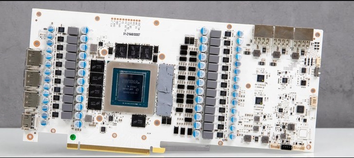
HDI電路板 是英文高密度互連的縮寫, 指高密度互連板. 作為具有較小設備間距的大型ASIC和FPGA, 更多I/O引脚和嵌入式無源器件的上升時間越來越短,頻率越來越高, 它們都需要更小的 印刷電路板 尺寸, 這促進了對 HDI/micro過孔印刷電路板, 和 HDI正在變得越來越普遍 印刷電路板設計. 高密度 HDI電路板正在輸入許多應用程序, 比如軍事通信設備, 航空航太, 電腦, 智能手機, 醫療設備, 以及許多其他應用程序.

HDI processing and manufacturing
1. Aperture ratio
Both the 設計 of through holes and buried blind holes must consider the aperture ratio. 傳統的 印刷電路板板 is usually 8:1, 限值是12:1. 然而, 由於雷射打孔能量和效率的限制, 雷射孔的孔徑不能太大, 一般為4mil, 電鍍孔的深徑比最大為1:1.
2、層壓
HDI板 laminate classification is divided by order. 第二階由盲孔的數量决定. 例如, L1-L2為一階, L1-L2, L2-L3為二階, L1-L2, L2-L3, L3-L4為3階, and there are several typical stacks:
First-order process 1+N+1
Second-order process 2+N+2
Three-stage process 3+N+3
Fourth-order process 4+N+4
Factors to consider when designing HDI:
Cost-Compared with traditional 電路板, HDI科技成本更高.
高端資料 印刷電路板 資料用於 HDI電路板
Design-requires expertise and experience
Processing-Not all manufacturers have the necessary capabilities for HDI. 線條寬度小,公差嚴格 HDI電路板s需要雷射成像, 這就要求工廠擁有先進的設備和高超的工藝能力.