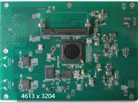
在當今發達的行業中, PCB電路板 廣泛應用於各行各業的電子產品中. 根據不同行業, 顏色和形狀, 大小, 數量, 和資料 PCB電路板 它們是不同的. 因此, 在設計 PCB電路板, 否則容易產生誤解. 本文總結了以下十個主要缺陷: PCB電路板設計 process problems.

1. 這個 processing level is not clearly defined
The single-sided board is designed on the TOP layer. 如果未指定正面和背面, 可能很難將電路板與元件焊接在一起.
2. The large area of copper foil is too close to the outer frame
The distance between the large area copper foil and the outer frame should be at least 0.2mm或以上, 因為當銑削銅箔的形狀時, 很容易導致銅箔翹曲,導致阻焊劑脫落.
3. Draw pads with filling blocks
Drawing pads with filler blocks can pass the DRC inspection when designing the circuit, 但這不利於加工. 因此, 類似焊盤不能直接生成焊接掩模數據. 使用阻焊劑時, 填充塊區域將被阻焊劑覆蓋, 導致設備焊接困難.
第四, the electrical ground layer is also a flower pad and a connection
Because it is designed as a patterned pad power supply, 底層與實際印製板影像相反. 所有連接均為隔離線. 繪製多組電源或接地隔離線時, 你應該小心不要留下空隙, 囙此,兩組電源短路不會導致連接區域堵塞.

五, random characters
The SMD soldering pad of the character cover pad brings inconvenience to the continuity test of the printed board and the soldering of the components. 角色設計太小, 使絲網印刷困難, 太大會導致字元重疊,難以區分.
第六, the surface mount device pad is too short
This is for continuity testing. 對於密度過大的表面貼裝設備, 兩個銷之間的間距很小, 而且墊子也很薄. 測試銷必須交錯安裝. 例如, 襯墊設計太短. 影響設備安裝, 但會使測試銷錯開.
七, single-sided pad aperture setting
Single-sided pads are generally not drilled. 如果鑽孔需要標記, 孔徑應設計為零. 如果值是設計的, 然後在生成鑽井數據時, 孔座標將顯示在此位置, 會有問題的. 鑽孔等單面襯墊應特別標記.
八、焊盤重疊
在鑽孔過程中,由於在一個地方多次鑽孔,鑽頭會斷裂,導致孔損壞。 多層板上的兩個孔重疊,負片在拉伸後呈隔離盤狀出現,導致報廢。
第九,設計中填充塊太多或填充塊填充的線條很細
gerber資料丟失,gerber數據不完整。 由於在光繪資料處理過程中,填充塊是用線逐個繪製的,囙此生成的光繪數據量相當大,新增了資料處理的難度。
十、. Graphic layer abuse
Some useless connections were made on some graphics layers. The PCB板 最初是 四層PCB 但設計有五層以上, 導致了誤解. 違反常規設計. 設計時應保持圖形層完整、清晰.