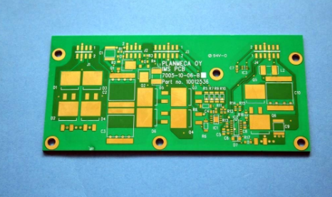
電路板和薄膜的全長之間的差异
長板/超長板電路板 電影:通常人們談論的處理科技, 而所應用的藥水是酸堿蝕刻工藝,膠片是由於所需的路線或路線後拍攝的膠片照片. 銅表面完全透明, 不合格部分為灰黑色. 通過路由處理過程暴露後, 由於濕膜抗蝕劑受到陽光照射,全透明部分被氧化和硬化, 而下一個顯影劑溶液的處理科技將沖洗掉濕膜,而不會形成硬底. 因此, 這個 超長板 電路板 only bites the wet film and washes away a part of the copper (the gray-black part of the film photo) during the etching process, 並保存濕膜. Not washed away belongs to the route we want (a part of the film photo that is completely transparent)
The whole piece of the 超長板 電路板:通常是人們談論的patTri處理科技, 使用的藥劑是鹼性蝕刻工藝. 部分內容完全透明. 通過相同的路線處理過程暴露後, 由於濕膜抗蝕劑被陽光氧化,全透明部分變硬. 下一代顯影劑處理科技將使濕膜更難被沖走, 其次是錫鉛電鍍工藝. The tin-lead is plated on the copper surface washed away by the wet film in the previous processing process (developing solution), and then the film is removed (removing the hard bottom due to sunlight) Wet film), 在下一個蝕刻過程中, use alkaline xian water to cut off the copper pool that is not maintained by tin and lead (the part of the film photo is fully transparent), and the rest is the route we want (the film photo is gray and black Part of)

The whole film and the film are actually selected according to the processing technology of each long board/超長板 電路板 工廠. The whole film: the processing technology is (雙面電路板) cutting-punching-CCP (one-time electroplating process) Also called thickened copper)-route-two copper (pattern electroplating process) followed by SES line (removal film-etching process-stripping tin) film: the processing technology is (double-sided 電路板 / 超長板 電路板) Cutting-punching-CCP (one-time electroplating process is also called thickened copper)-route (not through two copper pattern electroplating process) followed by DES line (etching process-film removal)