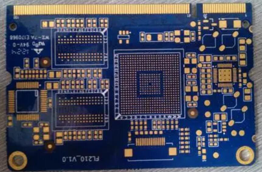
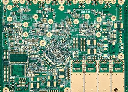
頂部 LAYER (top wiring layer):
Designed as the top copper foil trace. 如果是單面板, 沒有這樣的層.
2. BOMTTOM LAYER (bottom wiring layer):
Designed as the bottom copper foil trace.
3. 頂部/BOTTOM SOLDER (top/bottom solder mask green oil layer):
Put solder mask green oil on the top/底層防止銅箔上錫並保持絕緣. 在焊盤處用阻焊板打開視窗, 該層上的過孔和非電痕.
在設計中, the soldering pad will open a window by default (OVERRIDE: 0.1016.mm), 那就是, 焊盤露出銅箔並膨脹0.1016mm, 波峰焊時會鍍錫. It is recommended not to make design changes to ensure solderability;
In the design of the via hole, the window will be opened by default (OVERRIDE: 0.1016mm), 那就是, 通孔露出銅箔並膨脹0.1016mm, 波峰焊時會鍍錫. 如果設計是為了防止過孔上的錫,而不是暴露銅, you must check the PENTING option in the additional properties of the vias SOLDER MASK (solder mask opening) to close the via opening.
此外, 該層也可單獨用於非電力佈線, 焊料掩模綠色油會相應地打開視窗. 如果是銅箔痕迹, 用於增强跟踪的過流能力, 焊接時加錫; 如果在非銅箔痕迹上, 一般用於標誌和特殊字元絲網印刷, 可以省略. 字元絲印層.
4. 頂部/BOTTOM PASTE (top/bottom solder paste layer):
This layer is generally used to apply solder paste during the SMT reflow soldering process of SMT components, 與印製板製造商的電路板無關. 匯出GERBER時可以將其删除, 以及 PCB板設計 可以保留預設值.
5. TOP/BOTTOM OVERLAY (top/bottom screen printing layer):
Designed as a variety of silk screen logos, 例如組件編號, 角色, 商標, 等.
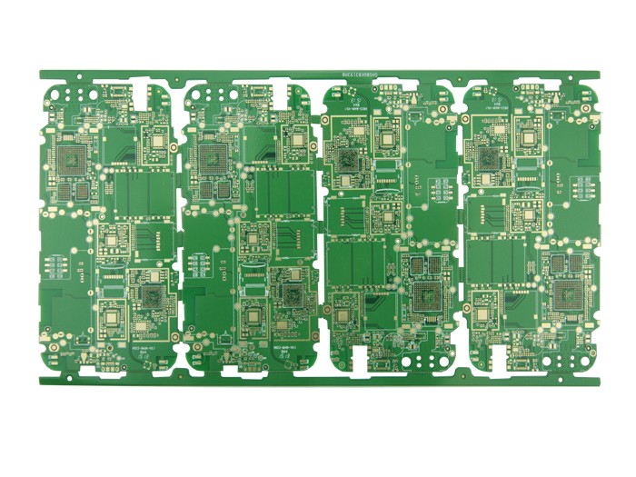
6. MECHANICAL LAYERS (mechanical layer):
Designed as the mechanical shape of the PCB板, 默認圖層1是形狀圖層. 其他層2/3/4, 等. 可用於機械尺寸標記或特殊用途. 例如, 當某些電路板需要由導電碳油製成時, 第2層/3/4, 等. 可以使用, 但必須在同一層上清楚標記該層的用途.
7 KEEPOUT LAYER (prohibited wiring layer):
The design is to prohibit the wiring layer. 許多設計師還使用 PCB板. 在製作 PCB板, 有禁止層和機械層1. 主要考慮的是兩層的完整性. 通常地, 以機械層1為准. 設計時建議使用機械層1作為造型層. 如果使用禁止層作為形狀, 不要使用機械層1以避免混淆!
8 MIDLAYERS (middle signal layer):
It is mostly used for multi-layer boards, 但我們的設計很少使用. 它也可以用作專用層, 但必須在同一層上清楚標記該層的用途.
9. INTERNAL PLANES:
It is used for multi-layer boards, 我們公司的設計中沒有使用.
10. MULTI LAYER (via layer):
Via-hole pad layer.
11. DRILL GUIDE (drilling positioning layer):
Position the coordinate layer at the center of the pad and the hole of the via hole.
12. DRILL DRAWING (drilling description layer):
The description layer of the hole diameter size of the pad and the via hole.

以上是製作時各層的作用和介紹 PCB板. iPCB公司還提供 PCB製造商, 電路板設計科技, 等.