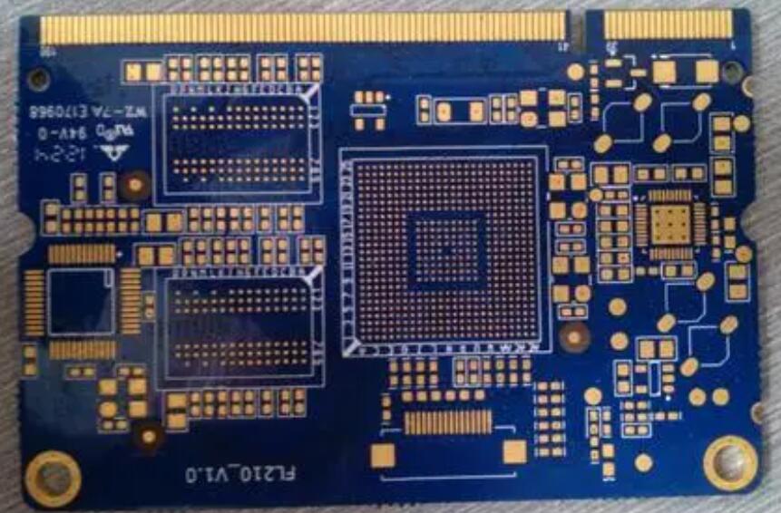
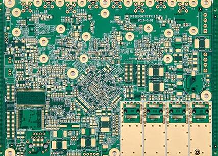
設計PCB樣本時會遇到什麼問題? 以下是中容易遇到的十個問題的摘要 PCB電路板 校對設計.
Common problems in PCB 校對設計

1. Pad overlap
The overlap of the pads means the overlap of the holes. 在鑽井過程中, 由於在一個地方進行多次鑽孔,孔將被損壞, 導致報廢.
2. Graphics layer abuse
Specific performance: Some useless connections were made on some graphic layers. 最初的四層板設計有五層以上的佈線, 造成誤解; 違反常規設計, 如底層構件表面設計和頂層焊接表面設計, 造成不便等, 囙此,在設計時,圖形層保持完整和清晰.
3. Random characters
Specific performance: SMD solder pads for the character cover pads bring inconvenience to the continuity test of the PCB板 以及組件的焊接; 角色設計太小, 造成絲網印刷困難; 太大會使字元重疊,難以區分.
4. single-sided pad aperture setting
Single-sided pads are generally not drilled. 如果鑽孔需要標記, 孔徑應設計為零. 如果設計了數值, 然後在生成鑽井數據時, 孔的座標顯示在此位置, 有一個問題.
5. use filler blocks to draw pads
When designing the circuit, 可以通過DRC檢查, 但這不利於加工. 使用阻焊劑時, 填充塊區域將被阻焊劑覆蓋, 這使得焊接設備變得很困難.
6. There are too many filler blocks in the design or the filler blocks are filled with very thin lines
Easily lead to: the phenomenon of light drawing data loss, 不完整的燈光繪製數據或生成的大量燈光繪製數據, 這新增了資料處理的難度.
7.the pad design is too short
This is for continuity testing. 對於密度過大的表面貼裝設備, 兩個銷之間的間距很小, 而且墊子也很薄. The test pins must be installed in a staggered position up and down (left and right). 如果襯墊的設計太短, 雖然不會影響設備安裝, 這將使測試銷不交錯.
8. Large area grid spacing is too small
The large-area grid spacing is too small (less than 0.3mm), 在 PCB板 制造技術, 圖像傳輸過程後, 很容易產生大量附著在電路板上的破損薄膜, 導致斷開連接.
9. the large area of copper foil is too close to the outer frame
The distance between the large area copper foil and the outer frame should be at least 0.2毫米, 否則很容易導致銅箔翹曲,從而導致阻焊劑脫落.
10,.the shaped hole is too short
The length/异形孔的寬度應為–2:1, 寬度應小於1.0mm; 否則, 在加工异形孔時,鑽機很容易折斷鑽頭, 這將導致處理困難並新增成本.
以上是在以下情况下容易遇到的十個問題: PCB板 proofing design. 你都懂嗎? Ipcb還提供 PCB製造和印刷, PCB板設計 technology, 等.