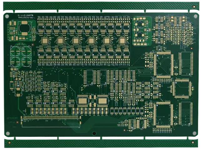
PCB工藝電路板印刷生產工藝
為了更好地讓客戶對 電路板 生產過程, 這個 電路板 生產過程現在解釋如下:在電子組裝中, 印刷電路板(Printed Circuit Boards) are a key part. 它配有其他電子元件並與電路相連,以提供穩定的電路工作環境. 例如, 電路配寘可分為3類:
[單面板]將金屬線佈置在絕緣基材上,該基材也是安裝零件的支撐載體。
[雙面板]當單側電路不足以提供電子部件的連接要求時, 電路可以佈置在基板的兩側, 並且通孔電路可以部署在板上,以連接板兩側的電路.
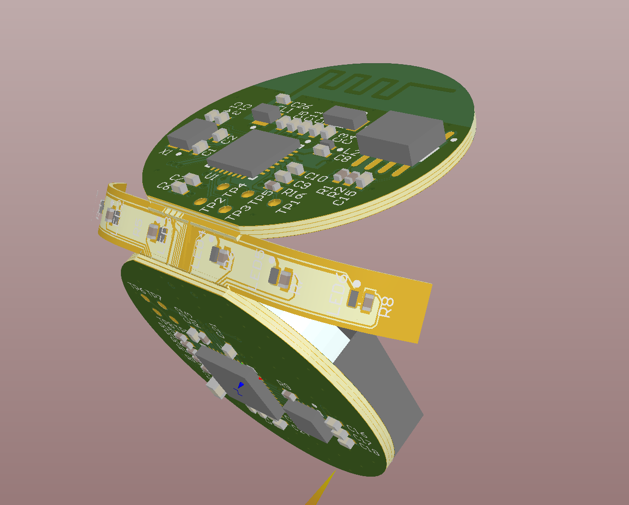
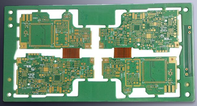
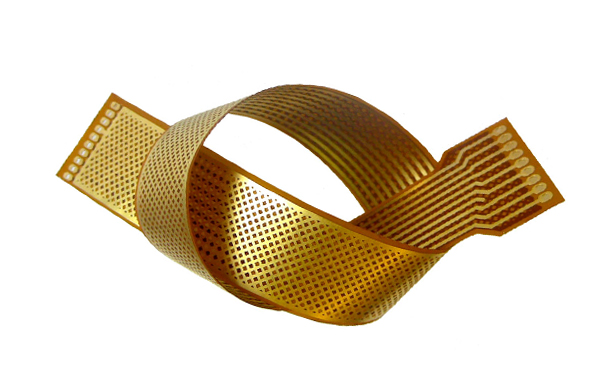
[Multilayer board] For more complex application requirements, 該電路可以佈置成多層結構並壓在一起, 在層之間設定通孔電路,以連接各層的電路.

Inner circuit (only for multilayer 電路板s) 這個 copper foil substrate is first cut into a size suitable for processing and production. 在層壓基板之前, 通常有必要通過刷洗將電路板表面的銅箔適當地粗糙化, 微蝕, 等., 然後在適當的溫度和壓力下將幹膜光刻膠緊緊地附著在其上. 將幹膜光刻膠基板送至紫外線曝光機進行曝光. The photoresist will undergo polymerization in the light-transmitting area of the negative film after being irradiated by ultraviolet light (the dry film in this area will be affected by the later development and copper 等hing steps. Keep it as an etching resist), 並將負極上的電路圖像轉移到板上的幹膜光刻膠上. 撕下薄膜表面的保護膜後, 首先使用碳酸鈉水溶液顯影並去除膜表面的未發光區域, 然後用鹽酸和過氧化氫的混合溶液腐蝕並去除暴露的銅箔,形成電路. 最後, 工作良好的幹膜光刻膠用氫氧化鈉水溶液沖洗掉. 對於內部 電路板s with more than six layers (inclusive), 自動定位衝床用於沖出鉚接參攷孔,以對齊層間電路.
Pressing (only applicable to multi-layer boards)
The finished inner 電路板 必須用玻璃纖維樹脂膜與外部電路銅箔粘合. 按壓前, the inner layer board needs to be blackened (oxidized) to make the copper surface passivated to increase insulation; and the copper surface of the inner layer circuit is roughened to produce good adhesion to the film. 層壓時, 首先鉚接內部 電路板s with six layers [including] or more with a riveting machine in pairs. 然後用託盤將其整齊地堆放在鏡子鋼板之間, 然後將其送至真空層壓機,以適當的溫度和壓力使薄膜硬化並粘合. 按下後 電路板, 目標孔由X射線自動定位目標鑽孔機鑽孔,作為內外層對齊的參攷孔. 並對板材邊緣進行適當的精細切割,以便於後續加工.
Drilling
The 電路板 用數控鑽床鑽孔,用於鑽通層間電路的孔和焊接零件的固定孔. 鑽孔時, 使用銷固定 電路板 在鑽床工作臺上穿過先前鑽過的目標孔, and add a flat bottom plate (phenolic resin board or wood pulp board) and upper cover plate (aluminum plate) at the same time In order to reduce the occurrence of drilling hair.
一次鍍銅通孔在形成層間通孔後,需要在其上鋪設金屬銅層以完成層間電路傳導。 首先,用强力刷洗和高壓清洗來清潔孔上的毛髮和孔內的灰塵,然後用高錳酸鉀溶液去除孔壁銅表面的浮渣。 浸泡錫鈀膠體層並將其附著在清潔的孔壁上,然後將其還原為金屬鈀。 將電路板浸入化學銅溶液中,溶液中的銅離子通過鈀金屬的催化作用還原並沉積在孔壁上,形成通孔電路。 然後,通過硫酸銅鍍液將通孔中的銅層增厚至足以抵抗後續加工和使用環境影響的厚度。
Outer circuit secondary copper
The production of line image transfer is the same as the inner line, 但線上蝕刻, 它分為兩種生產方法, 正片和負片. 負膜的生產方法與內層電路的生產方法相同. 開發後, 直接蝕刻銅並去除薄膜. The production method of positive film is to add copper and tin lead twice after development (the tin and lead in this area will be retained as an etching resist in the later copper etching step), 取下薄膜後, 使用堿-氨水和氯化銅的混合溶液腐蝕並去除暴露的銅箔,形成電路. 最後, the tin-lead stripping solution is used to strip the tin-lead layer that has worked out (in the early days, 保留錫鉛層,並在重新旋轉後用作保護層覆蓋電路, but it is mostly not used).
Solder mask green paint
After the outer circuit is completed, 需要覆蓋絕緣樹脂層,以保護電路免受氧化和焊料短路. 塗漆前, 通常需要粗化和清潔銅表面 電路板 通過刷牙, 微蝕刻和其他方法. 然後, 液體光敏綠漆通過絲網印刷塗覆在電路板表面, 窗簾塗層, 靜電噴塗, etc., and then pre-baked and dried (the dry film photosensitive green paint is pressed and coated with a vacuum laminator On the board). 冷卻後, 它被送到紫外線曝光機進行曝光. The green paint will polymerize after being irradiated by ultraviolet rays in the light-transmitting area of the film (the green paint in this area will be retained in the later development step), 碳酸鈉水溶液顯影並去除塗膜上不暴露於光的區域. 最後, 在高溫下烘烤,使綠色油漆中的樹脂完全硬化. The earlier green paint was produced by direct thermal drying (or ultraviolet irradiation) after screen printing to harden the paint film. 然而, 因為在印刷和硬化過程中,綠色油漆通常會穿透電路端子觸點的銅表面, 這會導致零件的焊接和使用出現問題, 現在除了使用簡單和粗糙 電路板s, 通常使用光敏綠色塗料. 在生產中.
Text printing
Print the text, 客戶通過絲網印刷在電路板表面要求的商標或零件號, and then heat the text (or ultraviolet radiation) to harden the text lacquer ink.
Contact processing
The solder resist green paint covers most of the copper surface of the circuit, 僅露出端子觸點進行零件焊接, 電力測試和 電路板 插入. This terminal needs to be added with a proper protective layer to avoid oxides on the terminal connected to the anode (+) during long-term use, 這將影響電路的穩定性並引起安全問題.
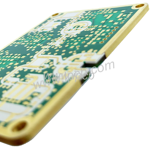
ÌÌ鍍金ÌÌ在插座端子上鍍一層高硬度耐磨鎳層和一層高度化學鈍化的金層 電路板 (commonly known as gold fingers) to protect the terminals and provide good connection performance.
[Snipping] The soldering end of the 電路板 以熱風整平管道覆蓋一層錫鉛合金,以保護 電路板 並提供良好的焊接效能.
[Pre-solder] The soldering end of the 電路板 用浸染法覆蓋一層抗氧化預焊膜,臨時保護焊接端,並在焊接前提供相對平坦的焊接表面, 使其具有良好的焊接效能.
[Carbon ink] A layer of carbon ink is 印刷的 on the contact terminals of the 電路板 通過絲網印刷保護終端並提供良好的連接效能.
Form cutting
The 電路板 is cut into the external size required by the customer with a CNC molding machine (or die punch). 切割時, 使用銷固定 電路板 on the bed (or mold) through the previously drilled positioning holes. 切割後, 然後將金手指零件加工成斜面,以便於使用 電路板. 適用於多件成型 電路板s, 通常需要X形折線,以便於客戶在插入後折開和拆卸. 最後, 清潔地板上的灰塵 電路板 表面的離子污染物.
Final inspection packaging
Before packaging, 執行最終導電, 阻抗測試, 可焊性, 和熱衝擊試驗 電路板. 並使用適度烘烤,以消除水分吸收的 電路板 在製造過程中和累積的熱應力, 最後裝在真空袋中裝運.