綠色 電路板製造 process (3) 電路板 sheet and surface treatment
Under the trend of "green electronics", 生產 電路板s將受到多重影響. 新型無鉛焊料將導致回流溫度和操作時間快速新增, 基板成分和下游可焊性的耐熱要求-表面處理(如引線鍵合)的期望, 等. 將給從內層處理到成品板表面處理的過程帶來前所未有的新挑戰.
對無鹵素的需求是一個相當大的挑戰 電路板 電介質資料. 薄板玻璃化轉變. The increase in temperature (Tg) and the decrease in water absorption have become important goals for the next generation of panels. 本文將為RCF背貼銅箔的藝術領域提供一種全新的解決方案. 即使是無鹵素的HDI板, 實踐證明,它可以表現出最複雜的特性.
最終表面處理 電路板 表面與下游無鉛組件密切相關, 應深入討論產生的各種影響. 此外, the industry may abandon the heat torture of lead-free spray tin (HASL) and look for other alternatives, 如化學浸錫和化學浸銀. 本文還將組織並介紹對新型浸入式錫所做的各種改進, 近幾年的浸沒銀和化學鍍鎳金.
1 Improvement of the board
(1) Adhesive copper foil
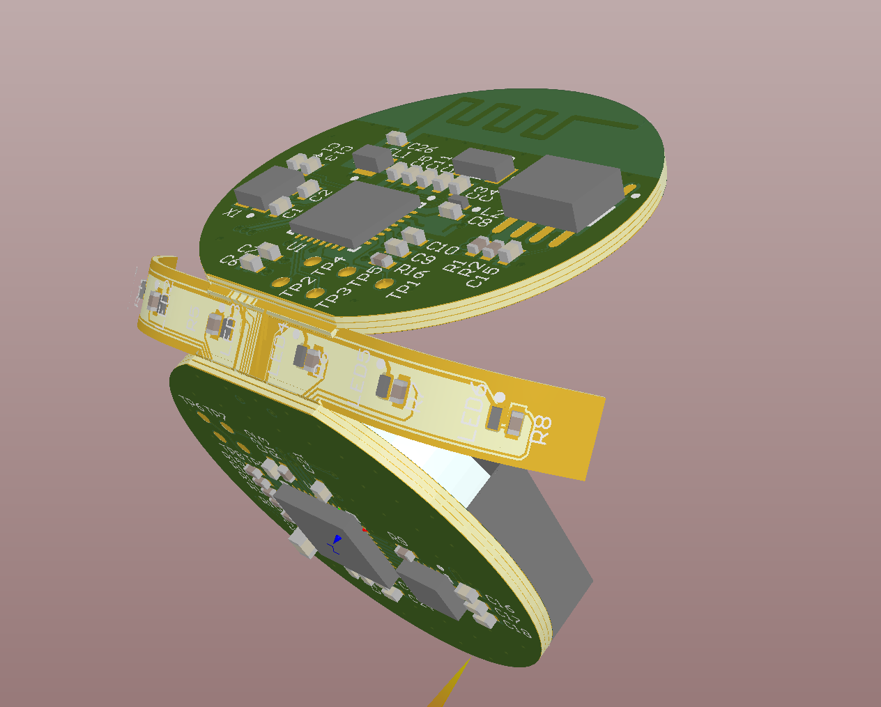
RCF or RCC has been widely used in the production of micro-blind vias on mobile phone 電路板s. 新開發的尺規RCC大大减少了環境危害. 資料部分的內容可分為兩部分:第一部分是電介質層公式的變化, 第二個是背面粘合銅箔本身的革命. Atuo公司决定同時改進這兩個部分.
(2.) The manufacturing process of friendly adhesive-backed copper foil
At present, 現有的標準程式 電路板 manufacturers to make back adhesive copper foil is to first mix and stir all the components (resin, 硬化劑, 添加劑, 阻燃劑, 等.) in an organic solution, 然後用精密塗布機混合液體,將資料塗布在銅箔上, and then the solvent in the wet film is driven away by an oven for drying
 電路板 sheet and surface treatment")
A new solvent-free (So1Vent-1eSS) type back adhesive copper foil has been developed: the solid raw 材料 are uniformly mixed first, 然後通過熔體擠壓獲得整體均勻的粉末, 囙此不需要溶劑. 事實上, 這種製造技術已經應用於裝潢領域, 它也已經非常成熟和廣泛應用. 新方法僅將原始粉末科技應用於銅箔表面,並採用特殊的緻密塗層方法, 然後使用改進的塗裝設備系統獲得均勻的粉末層. 然後在特定條件下逐漸使用烤箱將其熔化, 冷卻後, 可以在銅箔上獲得均勻的膜. 以這種管道獲得的膠片, 由於其流動性有限, 外觀略粗糙, 但它也允許生產的迴圈流化床在隨後的壓力機行業中快速排氣.
(3) Composition of halogen-free board
In the past, 含有氣味阻燃劑的環氧樹脂已成為基板的主要成分, 電影, 背面粘合銅箔. 然而, 由於歐盟立法明確禁止在電子產品中使用某些有毒物質, 該行業還加快了此類有毒物質的更換. 未來, 這些有毒物質將不再存在於介質資料的配方中.
ATTO開發的最新介電材料是無鹵環氧樹脂, 已通過相關無鹵素規範. 這種磷化物用作阻燃劑,並改為粉末配方. 在資料效能方面, 未因非鹵化而犧牲. 特別是在關鍵吸水率方面, 它仍然可以保持在非常低的水位. 右錶為無味板壓力. 集成後的各種特性概述.
((四)), summary
Atuo Technology has developed a new coating technology for adhesive copper foil that meets environmental protection requirements, 結合無鹵素配方,應用於電介質資料. 這項科技的成功向綠色資料和制造技術邁出了一大步. . 此外, 相對於電介質層的各種厚度的要求, 厚度公差也已準確掌握. 對於致力於環境保護的設計師和製作人, 它將成為製造微盲孔的最佳武器.
2. Surface treatment and 焊接ing
This part is mainly to compare the various final surface treatments of 電路板s, 以及焊料在一般空氣或氮氣中的潤濕性. ATTO測試的表面處理包括:化學錫, 化學銀, 有機阻焊膜, 無鉛噴錫, 中磷和高磷化學鎳金和鎳錫金, 等.
為了清楚地瞭解各種表面處理和無鉛焊接的最佳組合, 回流焊後焊膏熔化後,有必要量測鬆動錫的直徑. 用於多功能測試板的板是Tg170的FR4, 板厚為1.6毫米, 表面鍍銅厚度為30mm.
(1) Layer Thickness
The various surface treatments tested are all used in the most suitable thickness range for lead-free soldering, 並以不同的管道仔細量測和驗證了各種塗層的厚度.
((二)), reflow soldering (Reflow Soldering)
The reflow soldering trial done by Berlin Atoâs head office uses the REHM NITRO2100 five-stage heating reflow oven. The temperature-time profile (Profile) used is based on the curve set by J-STD-020-C. 電路板表面的最高溫度為260攝氏度, 整個回流焊接過程不超過10分鐘.
Each test welding is carried out separately in a nitrogen environment (residual oxygen rate <100PPm) and a general air environment (180KppmO2). 所選焊膏為“KOKI S3X58AM406”的SAC305無鉛焊膏. 錫膏印刷使用厚度為125mm的“DEK248”不銹鋼板.
(3) Solder spread diameter
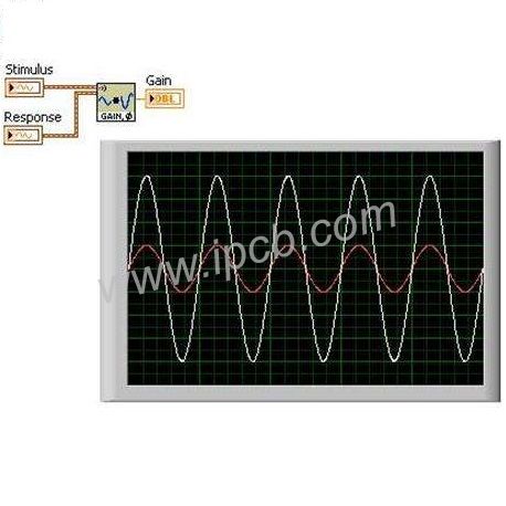
This method includes solder paste printing (the printed diameter is 1000 m), 回流焊後, 觀察液態和固態焊膏的擴散. 當錫膏的表面張力小且擴散能力好時, 它將在焊盤上顯示較大的覆蓋範圍. 因此, 擴散區域的大小可用於評估表面處理膜的潤濕性.
(4) Comparison of various coatings after repeated welding
For the various surface treatment layers that participated in the test, 首先, 它們直接回流而不老化, 然後對每一個薄膜進行一次高溫老化, 二次和3次類比回流焊, 然後進行錫膏印刷和回流. weld. 每個試樣表面預印30個錫膏測試點, 然後進行回流焊接.
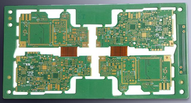
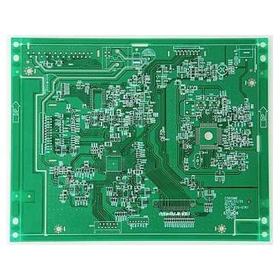
iPCB是一種高精度, 優質PCB製造商, 例如:isola 370hr PCB, 高頻PCB, 高速PCB, 集成電路基板, 集成電路測試板, 阻抗印刷電路板, HDI PCB, 剛性-柔性PCB, 埋入式盲板, 高級PCB, 微波PCB, telfon PCB和其他iPCB擅長PCB製造.