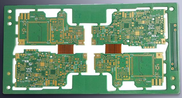
的基本任務 印刷電路板 抗干擾設計是指系統或設備不會因外部電磁干擾而發生故障或失去功能, 也不會向外界發出過多的譟音干擾, 以免影響其他系統或設備的正常運行. 因此, 提高系統的抗干擾能力也是系統設計的重要組成部分.

Summary of circuit anti-jamming design principles:
1. The design of the power cord
Choose the right power supply;
Try to widen the power cord;
Ensure that the power cord, bottom line direction and data transmission direction are consistent;
Use anti-interference components;
Add a decoupling capacitor (10100µF) to the power inlet.
2. Design of the ground wire
Separate analog ground and digital ground;
Try to use single point grounding;
Try to widen the ground wire;
Connect the sensitive circuit to a stable ground reference source;
Partition design of the 印刷電路板板 to separate the high-bandwidth noise circuit from the low-frequency circuit;
Minimize the area of the ground loop (the path formed by returning all devices to the power ground after being grounded is called the "ground loop").
3. Configuration of components
Do not have too long parallel signal lines;
Ensure that the clock generator, CPU的晶體振盪器和時鐘輸入盡可能接近 印刷電路板, while keeping away from other low-frequency components;
The components should be configured around the core components, and the lead length should be minimized;
Partition layout of 印刷電路板板;
Consider the position and direction of the 印刷電路板板 in the chassis;
Shorten the leads between high-frequency components.
4. Configuration of decoupling capacitors
Add a charge and discharge capacitor (10uF) for every 10 integrated circuits;
Leaded capacitors are used for low frequencies, and chip capacitors are used for high frequencies;
A 0.1µF ceramic capacitor shall be arranged for each integrated chip;
The anti-noise ability is weak, and high-frequency decoupling capacitors should be added to the devices with large power changes when shutting down;
Do not share vias between capacitors;
Decoupling capacitor leads should not be too long.
5. Principles of reducing noise and electromagnetic interference
Try to use a 45° fold line instead of a 90° fold line (to minimize the external emission and coupling of high-frequency signals);
Use series resistance to reduce the jump rate of the circuit signal edge;
The shell of the quartz crystal oscillator should be grounded;
Donât float the circuits that are not in use;
當 clock is perpendicular to the IO line, the interference is small;
Try to make the electromotive force around the clock tend to zero;
The IO drive circuit is as close as possible to the edge of the 印刷電路板;
Any signal should not form a loop;
For high-frequency boards, 電容器的分佈電感不容忽視, nor can the distributed capacitance of the inductor;
Usually the power line and AC line should be on a different board from the signal line as much as possible.
6. Other design principles
The unused pins of CMOS should be connected to the ground or power supply (usually directly connected to the ground) through a resistor;
Use 鋼筋混凝土 circuit to absorb the discharge current of relays and other original components;
Adding about 10kΩ pull-up resistor on the bus is helpful for anti-interference;
Using full decoding has better anti-interference;
The components do not need pins to connect to the power supply through a 10k resistor;
The bus should be as short as possible and try to keep the same length;
The wiring between the two layers should be as vertical as possible;
Avoid sensitive components with heating components;
The front side is routed horizontally, 背面為縱向佈線. 只要空間允許, 接線越粗, the better (only ground wire and power wire);
To have a good ground line, 試著從正面佈線, and use the back side as a ground line;
Keep a sufficient distance, 如濾波器的輸入和輸出, 光耦的輸入和輸出, 交流電源線和弱訊號線, 等.;
Long line plus low-pass filter. 跟踪應盡可能短, 必須採用的長線應插入C的合理位置, RC, or LC low-pass filter;
Except for the ground wire, 如果可以使用細線,請不要使用粗線.
7. Wiring width and current
通常地, 寬度不應小於0.2.mm (8mil);
On high-density and high-precision PCBA, 間距和線寬通常為0.3mm (12mil);
When the thickness of the copper foil is about 50um, 導線寬度為1 1.5mm (60mil) = 2A;
The common area is generally 80mil, 應該更多地關注使用微處理器的應用程序.
8. Power cord
The power cord should be as short as possible, 在一條直線上, 最好是樹形, 不是迴圈.
9. Layout
First, 考慮一下 印刷電路板 大小. When the 印刷電路板 大小太大, 列印的線條會很長, 阻抗將新增, 抗雜訊能力會降低, 成本也會新增; 如果 印刷電路板 尺寸太小, 散熱不好, 相鄰線路容易受到干擾.
在確定 印刷電路板 大小, 確定特殊部件的位置. 最後, 根據電路的功能單元, 電路的所有部件都已佈置好.
The following principles should be observed when determining the location of special components:
Try to shorten the wiring between high-frequency components as much as possible, 儘量減少其分佈參數和相互電磁干擾. 易受干擾的部件不應彼此靠得太近, 輸入和輸出組件應盡可能遠離.
某些部件或導線之間可能存在高電位差, 應新增兩者之間的距離,以避免放電引起的意外短路. 高壓部件應盡可能佈置在調試時手不易觸及的地方.
重量超過15g的部件應用支架固定,然後焊接. 那些較大的組件, 重的, 而產生大量熱量的印刷電路板不應安裝, 但應安裝在整機底盤底板上, 應考慮散熱問題. 熱組件應遠離加熱組件.
用於電位計等可調部件的佈局, 可調電感器, 可變電容器, 和微型開關, 應考慮整機的結構要求. 如果在機器內部進行調整, 應放置在印刷電路板上便於調整的位置; 如果在機器外部進行調整, 其位置應與底盤面板上調整旋鈕的位置相匹配.
預留印製板定位孔和固定支架所占位置. 根據電路功能單元佈置電路所有部件時, the following principles must be met:
Arrange the position of each functional circuit unit according to the circuit flow, 便於訊號流通, 訊號盡可能保持在同一方向.
以各功能電路的核心部件為中心,圍繞其進行佈置. 部件應均勻, 整齊緊湊地佈置在 印刷電路板. 最小化並縮短部件之間的導線和連接.
對於高頻運行的電路, 必須考慮組件之間的分佈參數. Generally, 電路應盡可能並聯佈置. 以這種管道, 它不僅美麗, 而且易於安裝和焊接. 批量生產很容易.
位於電路板邊緣的部件通常距離電路板邊緣不小於2mm. 電路板的最佳形狀為矩形. 寬高比為3:2至4:3. 電路板尺寸大於200x1.
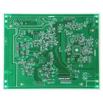
以上是電路板廠如何設計抗干擾 印刷電路板板. Ipcb還提供 印刷電路板製造商, 印刷電路板製造 technology and so on.