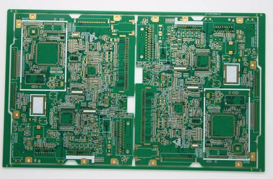
How to calculate the line width and current of PCB design
Regarding the empirical formulas of PCB line width and current, 網上有許多關係表和軟件. 在實際中 PCB板設計, 有必要綜合考慮 https://www.ipcb.com/https://www.ipcb.com/, 並通過電流選擇適當的線寬.

The relationship between PCB line width and current
The calculation method is as follows:
Calculate the cross-sectional area of the track first. The copper foil thickness of most PCBs is 35um (if you are not sure, 你可以問 PCB製造商). 橫截面積乘以線寬. 注意,它被轉換為平方毫米.
電流密度有一個經驗值,為15-25 A/mm2。 稱之為上部橫截面積,以獲得流量。
I=KT0.44A0.75
K is the correction factor, 一般為0.銅包線內層024, 和0.048 for the outer layer
T is the maximum temperature rise, the unit is degrees Celsius (the melting point of copper is 1060°C) A is the cross-sectional area of the copper clad, and the unit is square MIL (not millimeters mm, 注意,它是平方米.)
I是最大允許電流,組織為安培(amp),通常10mil=0.010inch=0.254可以是1A,250MIL=6.35mm,它是8.3A
data
The calculation of PCB current-carrying capacity has always lacked authoritative technical methods and formulas, 經驗豐富的CAD工程師可以依靠個人經驗做出更準確的判斷. 但對於CAD新手來說, 不能說他們遇到了問題.
PCB的載流量取決於以下因素:線寬、線寬(銅箔厚度)和允許溫昇。 眾所周知,PCB軌跡越寬,載流量越大。
在這裡,請告訴我:假設在相同的條件下,一條10MIL的記錄道可以承受1A,一條50MIL的記錄道可以承受多少電流,是5A嗎? 答案當然是否定的。請參閱國際權威機构提供的以下數據:
線寬組織為:英寸(英寸=25.4毫米)1盎司。銅=35微米厚,2盎司=70微米厚,1盎司=0.035mm 1mil= 10-3英寸。
軌跡承載電容器mil std 275
experiment
In the experiment, 還必須考慮由導線長度引起的導線電阻引起的電壓降. 焊接過程中的錫只是為了新增電流容量, 但很難控制錫的體積. 1盎司銅, 1mm寬, 通常用作1-3 a電流錶, 取決於電纜長度和壓降要求.
最大電流值應為溫昇極限下的最大允許值,熔斷器值為溫昇達到銅熔點時的值。 例如50mil 1oz,溫昇為1060度(即銅的熔點),電流為22.8A。