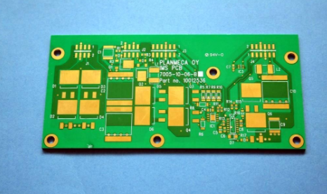
在 PCB電路板, the difference between the PCB板製造資料 鎳金和電鎳金如下.不同的 PCB製造商 使用不同的資料.

1. Different processes
Immersion nickel gold process: firstly deposit about 120-200m" thick nickel layer on the copper surface by autocatalytic reaction, 然後在金柱中通過化學置換反應將金從溶液中置換到鎳表面, 金層將完全覆蓋鎳層, 其厚度一般控制在1-3m”左右. 通過時間和其他控制,其厚度上限可高達10m“. 電鎳-金工藝:通過通電,在銅表面電化學鍍上一層約120-200m”厚的鎳. 鍍有一層約0.5-1m“厚薄金. 通過控制時間和電流,厚度可高達50m”或更大. 通過化學沉積,浸沒鎳金具有非常均勻的厚度, 而電鍍鎳金的厚度均勻性較差. 2. Different signal transmission capabilities
The electro-nickel-gold process uses a nickel-gold layer as a resist layer, 那就是, 所有線路和焊盤上都將有鎳金層. 高頻訊號傳輸基本上通過鎳金層, “皮膚效應”是乾燥的. 偏轉將嚴重影響訊號傳輸. 浸入式鎳金工藝僅在焊盤上有鎳金層, 線路上沒有鎳金層, 訊號將在銅層上傳輸. 其在集膚效應下的訊號傳輸能力遠遠優於鎳層.
3. Different process capabilities
The electro-nickel-gold process uses a nickel-gold layer as a resist layer. 蝕刻後, 賽道一側有一個鎳金懸挑. 這種懸挑很容易坍塌和斷裂,形成短路. 銅越厚, 風險越高, 非常不適合密集電路設計. 鎳金工藝是在電路和焊接掩模形成後生產的. 鎳金層僅附著在焊盤表面. 焊接掩模下的緻密電路沒有鎳金層, 囙此不會影響密集電路設計.
4. Different coating structure
The electro-nickel-gold process has fine and regular crystals of the nickel-gold layer coating, 而鎳金工藝的晶粒較大,為非晶態.
5. Different coating hardness
Use the micro Vickers hardness tester to test the hardness of the gold and nickel coatings of the two treatment methods. 無論是金層還是鎳層, 電鎳金高於浸沒鎳金, 金鍍層比鎳鍍層高7%左右. 大約高出24%.
6. Different solderability and wetting
According to the method specified in the standard IPC/J-STD-003B《印制板可焊性技術要求》, 進行了焊料潤濕性試驗, and the wetting time (zero-crossing time) of the two samples was basically the same. 然而, 隨著焊接的繼續, 浸沒鎳金的潤濕速度快於電鎳金. 原因是一方面, 鎳-金浸漬過程中的結晶顆粒粗糙且無定形, 使溶解和擴散更快. 另一方面, 塗層的硬度也是影響潤濕性的重要因素. 隨著硬度的新增, 潤濕性將逐漸降低. .
7. Different reliability risks
The immersion nickel gold process has a certain porosity due to the coarse and amorphous crystals in its structure. 氣孔會導致氧化,鎳層不會得到有效保護和腐蝕. 所謂的黑鎳需要新增金層的厚度來補償. 由於鍍層結晶良好, 電鎳金工藝一般不會出現黑鎳現象, 可靠性高. 金層的厚度僅為浸沒鎳金層厚度的一半甚至更薄.