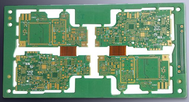
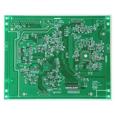
電路板設計 specification of switching power supply
In any switching power supply design, 的物理設計 PCB電路板 是最後一個連結. 如果設計方法不當, 這個 電路板 可能會輻射過多的電磁干擾,導致電源工作不穩定. The following is the attention required in each step The matters are analyzed:
1. 從示意圖到 電路板 Establish component parameters -> input principle netlist -> design parameter settings -> manual layout -> manual wiring -> verify design -> review -> CAM output.
2 參數設置相鄰導線之間的距離必須能够滿足電氣安全要求, 為了便於操作和生產, 距離應盡可能寬. 最小間距必須至少適合耐受電壓. 佈線密度低時, 訊號線的間距可以適當新增. 對於高電平和低電平之間存在較大間隙的訊號線, 間距應盡可能短,並應新增間距. 通常地, 將記錄道間距設定為8mil. 襯墊內孔邊緣與印製板邊緣之間的距離應大於1mm, 可以避免焊盤在加工過程中出現缺陷. 當連接到焊盤的痕迹很薄時, 焊盤和痕迹之間的連接應設計成滴狀. 這樣做的優點是墊子不容易剝離, 但是痕迹和焊盤不容易斷開.
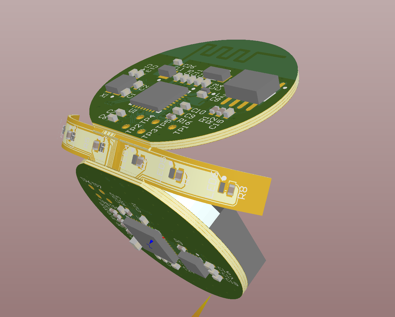
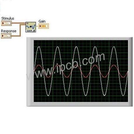
第3, 元件佈局實踐證明,即使電路原理圖設計正確,列印出的 電路板 設計不當, 這將對電子設備的可靠性產生不利影響. 例如, 如果印製板的兩條細平行線靠得很近, 這將導致訊號波形延遲和傳輸線終端的反射雜訊. 效能下降, 所以在設計印刷品時 電路板, 你應該注意採取正確的方法. Each switching power supply has four current loops:
· (1). Power switch AC circuit
· (2). Output rectifier AC circuit
· (3). Input signal source current loop
· (4). Output load current loop

The input circuit charges the input capacitor through an approximate DC current, 濾波電容器主要用作寬帶儲能; 同樣地, 輸出濾波電容器還用於存儲來自輸出整流器的高頻能量,並消除輸出負載電路的直流能量. . 因此, 輸入和輸出濾波電容器的端子非常重要. 輸入和輸出電流回路只能分別從濾波電容器的端子連接到電源; 如果輸入之間的連接/輸出回路和電源開關/整流器回路不能連接到電容器端子直接連接, 交流能量將通過輸入或輸出濾波電容器輻射到環境中. 電源開關的交流電路和整流器的交流電路包含高幅值梯形電流. 這些電流的諧波分量非常高. 頻率遠大於開關的基頻. 峰值振幅可高達連續輸入振幅的5倍/輸出直流電流. 過渡時間通常約為50ns. 這兩個回路最容易受到電磁干擾, 囙此,這些交流回路必須在電源中的其他印刷線路之前佈置. 每個回路的3個主要部件是濾波電容器, 電源開關或整流器, 電感器或變壓器. 將它們相鄰放置,並調整組件的位置,使它們之間的電流路徑盡可能短. 建立開關電源佈局的最佳方法類似於其電力設計. The best design process is as follows:
· Place the transformer
· Design the power switch current loop
· Design output rectifier current loop
· Control circuit connected to AC power circuit
· Design input current source loop and input filter
When designing the output load loop and output filter according to the functional unit of the circuit, 在佈置電路的所有部件時, the following principles must be met:
(1) First, 考慮 電路板. 當 電路板 太大了, 列印的線條會很長, 阻抗將新增, 抗雜訊能力會降低, 成本會新增; 如果 電路板 太小了, 散熱不好, 相鄰線路容易受到干擾. 最佳形狀的 電路板 是矩形的, 縱橫比為3:2或4:3. 位於 電路板 通常距離邊緣不小於2mm 電路板.
(2) When placing the device, 考慮後續焊接, 不太密集.
(3) Take the core component of each functional circuit as the center and lay out around it. 部件應均勻排列, 表面整潔緊湊 電路板, 最小化並縮短部件之間的導線和連接, and the decoupling capacitor should be as close as possible to the VCC of the device
(4) For circuits operating at high frequencies, 應考慮組件之間的分佈參數. 通常地, 電路應盡可能並聯佈置. 以這種管道, 它不僅美麗, 而且易於安裝和焊接, 易於批量生產.
(5) Arrange the position of each functional circuit unit according to the circuit flow, 這樣佈局便於訊號流通, 訊號盡可能保持在同一方向.
(6) The first principle of the layout is to ensure the wiring rate, 移動設備時,注意飛線的連接, 並將具有連接關係的設備放在一起.
(7) Reduce the loop area as much as possible to suppress the radiation interference of the switching power supply