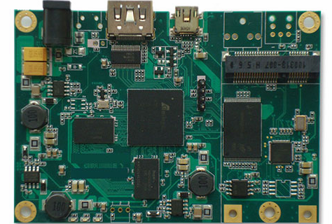
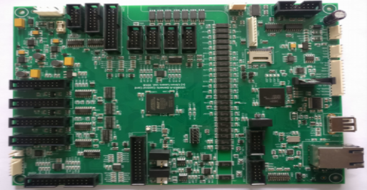
印刷電路板 process allows traditional plug-ins of through-hole components to also go through the reflow furnace process
Through-hole solder paste is to print the solder paste directly on the PTH (Plating Through Hole) of the 印刷電路板 (印刷電路板), 然後直接插入傳統挿件/through-hole components (DIP insert parts) Insert the electroplated through holes that have been printed with solder paste. 此時, 電鍍通孔上的大多數焊膏將粘附在挿件的焊脚上. 回流焊爐高溫後,這些錫膏將重新熔化, 然後焊接. 零件在 電路板.
此方法還有其他名稱,例如粘貼中的pin, 侵入式回流焊, and ROT (reflow of through-hole).
The advantage of this method is that it can eliminate the manual soldering (hand soldering) or wave soldering (Wave Soldering) process, thereby saving labor (Labor), 同時可以提高焊接質量, reduce the chance of solder short (Solder short).
然而, this construction method has the following inherent limitations:
The heat resistance of traditional parts must meet the temperature requirements of reflow soldering. 一般插入式零件通常使用比回流焊零件耐溫性低的資料. 因為這種方法要求傳統零件與普通SMT零件一起回流, 它必須滿足回流焊的耐溫性要求. Lead-free parts must now be able to withstand 260°C+10sec.
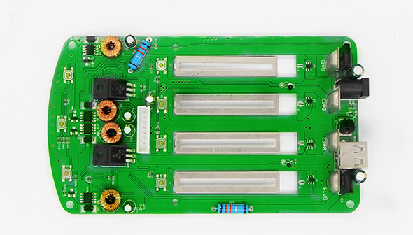
The parts are best to have tape-on-reel packaging (tape-on-reel) and enough flat surface can be put on the 電路板(印刷電路板) through the SMT automatic pick and place machine (pick and place machine), 如果沒有, 考慮另派一名操作員手動放置零件. 此時, 必須量測所需的工時和質量不穩定性, 因為手動挿件可能會接觸到由於操作不慎而放置和定位的其他零件.

零件主體和印刷電路板的焊盤必須具有隔離(提升)設計。 通常,PIH工藝會列印比焊盤外框大的錫膏。 這是為了新增錫膏焊料的數量,以達到通孔填充要求的75%。 如果零件和焊盤之間沒有焊距,則通過回流,熔融的焊膏將沿著零件和印刷電路板之間的間隙移動,形成雨錫渣和錫珠,這將影響未來的電力質量。
Traditional parts are best printed on the second side (if there are two-sided SMT). 如果零件已首先在第一面列印, 當SMD在第二側繼續時, 焊膏可能流回傳統零件, 導致內部短路的可能性, 尤其是連接器零件. 仔細的.
此外,焊料量是該方法的最大挑戰。 通孔焊點IPC-610的可接受標準焊料量必須大於載體板厚度的75%。
至於錫膏量的計算, 可以從通孔的最大直徑中减去銷的最小直徑, 然後將其乘以 電路板 為了得到它. 再次記住x2, 因為焊膏中的助焊劑占50%, 這是在回流焊之後, 也就是說, 錫膏的體積僅為原印刷錫膏的一半.
所需的錫膏體積大於或等於(通孔的最大直徑和引脚的最小直徑)/2]2*2*2*2*2電路板的厚度。
如何新增焊料量? The following methods are provided for your reference:
Reserve enough space near the through hole (PTH) of the 電路板 用於套印.
與佈線工程師討論,在需要在孔中粘貼的通孔附近留出更多空間列印焊膏,也就是說,儘量不要在附近放置其他焊盤或其他不需要的焊膏通孔。, 避免過度列印時短路。
應該注意的是,錫膏印刷的平面空間不能無限延伸, 必須考慮錫膏的粘合能力, 否則,錫膏將無法完全縮回焊盤並形成焊珠.
此外, 考慮錫膏印刷的方向必須與焊盤延伸的方向匹配.
减小上通孔的直徑 電路板.
就像上面計算所需的錫膏量一樣, 通孔直徑越大, 所需的錫膏量越多, 但同時, 如果通孔的直徑太小,則應考慮, 零件將插入通孔中.
Use step-up (local thickening) or step-down (local thinning) stencil (steel plate).
這種鋼板可以局部強制新增焊膏的厚度, 這也會新增錫膏的用量, 從而達到用焊料填充通孔的目的. 然而, 這種鋼板平均比普通鋼板貴10%.
調整適當的焊膏, 印刷機的速度和壓力, 刮刀的類型和角度, 等.
錫膏打印機的這些參數或多或少會影響錫膏列印量, and the solder paste with lower Viscosity (viscosity) will have more solder paste volume.
添加一些焊膏.
您可以考慮使用分配器在孔內焊盤上添加一些錫膏,以新增錫膏的數量. 因為現在幾乎所有的SMT生產線都沒有自動分配器, 您也可以考慮手動分配., 但有必要新增操作員的工作時間.
使用焊料預製件。