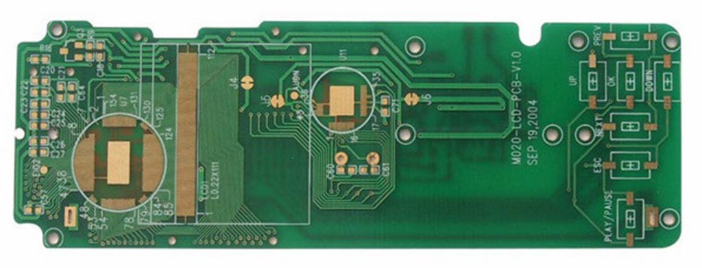
在中可能會遇到各種問題 印刷電路板打樣 過程. 作為一個 印刷電路板打樣製造商, 您需要注意 印刷電路板打樣 process:

1) The distance from the edge of the pad hole to the edge of the 印刷電路板板 對於 印刷電路板打樣 大於1mm, 可避免焊接板在加工過程中出現缺陷.
預防措施 印刷電路板打樣 are as follows:
1) The distance from the edge of the pad hole to the edge of the 印刷電路板板 對於 印刷電路板打樣 大於1mm, 可避免焊接板在加工過程中出現缺陷.
2) The pad is torn. 當連接到焊盤的銅膜線很薄時, 焊盤和銅膜線之間的連接應設計為淚滴狀, 使襯墊不易脫落, 銅膜線和導線之間的連接不容易斷開.
3) Adjacent pads should avoid sharp corners.
大面積填充的目的是在 印刷電路板 是兩個, 一是散熱, 二是减少遮罩干擾, 印刷電路板打樣 避免產生熱量, 從而排出電路板產生的氣體,剝離銅膜. 填充大面積的視窗, 後者使填充物成為網格.
使用銅還可以達到抗干擾的目的, 銅可以自動繞過焊盤,並可以接地.
印刷電路板板 單面電纜設計中的交叉佈線 印刷電路板板, 當某些銅膜無法連接時, 通常的方法是使用交叉接線. 交叉佈線的長度應選擇如下:6mm, 8mm和10mm.
印刷電路板板 high frequency wiring
To make the design of the 高頻印刷電路板板 更合理,抗干擾效能更好, 以下方面應在 印刷電路板板設計:
1) Reasonably choose the number of layers for 印刷電路板打樣
使用中間內平面作為電源和接地層, 它可以起到遮罩作用, 有效降低寄生電感, 縮短訊號線長度, 减少訊號之間的交叉干擾. 一般來說, 四層板的雜訊比兩層板低20dB.
2) 印刷電路板打樣 walking line mode
The wiring must be rotated at an angle of 45°, 可以减少高頻訊號的發射和互耦.
3) 印刷電路板校對接線 length
The shorter the line length, 更好的, 兩條線之間的平行距離越短, 更好的.
4) Number of holes
The fewer holes the better.
5) Interlayer wiring direction
When 印刷電路板打樣, 層間佈線方向應垂直, 那就是, 頂層為水准方向, 底部是垂直方向, 可以减少訊號之間的干擾.
6) Copper coating
Adding a grounded copper coating can reduce interference between signals.
7) Place of parcel
The grouping processing of important signal lines for 印刷電路板打樣 能顯著提高訊號的抗干擾能力. 當然, 可以對干擾源進行包裝,使其不會干擾其他訊號.
8) Signal cable
The signal wiring cannot be looped and needs to be wired according to the daisy chain mode. 深圳是生產量最大的都市 印刷電路板電路板 in China. 什麼是深圳 印刷電路板打樣 公司?
9) Decoupling capacitor
The cross decoupling capacitor is connected to the power supply terminal of the integrated circuit.
10) High-frequency choke digital, 類比和其他連接連接至高頻阻風門裝置的公共接地線, 以及 印刷電路板打樣 通常通過高頻鐵氧體磁珠和導線的中心孔.