佈線工程師談論 印刷電路板設計 經驗
印刷電路板 佈線科技——佈線工程師談 印刷電路板設計 experience
這個 general 印刷電路板 design process is as follows: preliminary preparation -> 印刷電路板 結構設計 -> 印刷電路板 佈局 -> wiring -> wiring optimization and silk screen printing -> network and DRC inspection and structure inspection -> plate making. "
First: Preliminary preparation. 這包括準備元件庫和示意圖. “如果你想做好, 你必須先磨快你的工具.“做一塊好木板, 除了設計原則, 你也必須畫得好. 繼續之前 印刷電路板設計, 我們必須首先準備原理圖SCH的組件庫和 印刷電路板. 組件庫可以使用Peotel自己的庫, 但通常很難找到合適的. 最好根據所選設備的標準尺寸數據創建自己的組件庫. 原則上, 執行 印刷電路板 首先是組件庫, 然後執行SCH組件庫. The 印刷電路板組件 library requirements are high, 直接影響板的安裝; SCH組件庫要求相對寬鬆, 只要注意管脚内容的定義以及與 印刷電路板組件. PS:注意標準庫中的隱藏管脚. 然後是原理圖的設計, 當它完成時, 已準備好啟動 印刷電路板設計.

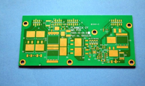
第二個: 印刷電路板 structure design. 在此步驟中, 繪製 印刷電路板表面 in the 印刷電路板設計 根據確定的 電路板 尺寸和各種機械定位, 並放置所需的接頭, 按鈕/開關, 螺釘孔, 裝配孔, 等. 根據定位要求. And fully consider and determine the wiring area and non-wiring area (such as how much area around the screw hole belongs to the non-wiring area).
第3: 印刷電路板 layout. 簡單地說, 佈局是將設備放置在電路板上. 此時, 如果上述所有準備工作都已完成, you can generate the netlist (Design->Create Netlist) on the schematic, and then import the netlist (Design->Load Nets) on the 印刷電路板 簡圖. 您可以看到整個設備堆棧崩潰, 針腳之間有飛線表示連接. 然後你可以佈置設備. The general layout is carried out according to the following principles:
1. . 根據電力效能的合理劃分, it is generally divided into: digital circuit area (that is, afraid of interference and interference), analog circuit area (fear of interference), power drive area (interference source)
2. . 完成相同功能的電路應盡可能靠近, and the 組件 should be adjusted to ensure the most concise connection; at the same time, adjust the relative position between the functional blocks to make the connection between the functional blocks the most concise;
3. 對於高品質組件, 應考慮安裝位置和安裝强度; 加熱部件應與溫度敏感部件分開放置, and heat convection measures should be considered when necessary;
4. ê/O drive device is as close as possible to the edge of the printed board and to the lead-out connector;
5. The clock generator (such as crystal oscillator or clock oscillator) should be as close as possible to the device that uses the clock;
6. . 各集成電路電源輸入引脚與接地之間, a decoupling capacitor (generally a monolithic capacitor with good high-frequency performance is used); when the board space is dense, 還可以在幾個集成電路鉭電容器周圍添加一個.
7. . A discharge diode should be added to the relay coil
8. . 佈局要求應平衡, 密集有序, not top-heavy or heavy
--Special attention is needed. 放置零部件時, the actual size of the components (occupied area and height) and the relative position between the components must be considered to ensure the electrical performance of the 電路板 並且生產的可行性和安裝的同時也很方便, 應在確保上述原則能够得到反映的前提下,對組件的放置進行適當修改,使其整潔美觀. 例如, 相同的部件應整齊地放置在同一方向上.
這一步與電路板的整體影像和下一步佈線的難度有關, 囙此,必須考慮一點努力. 佈局時, 您可以進行初步佈線,並充分考慮不確定的地方.