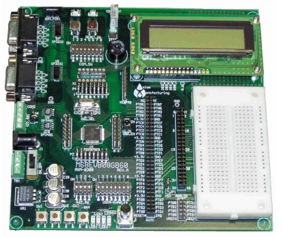
什麼 印刷電路板 engineers need to pay attention to
Many 印刷電路板 工程師經常繪製電腦主機板,並且非常精通allegro等優秀工具. 然而, 遺憾的是,他們很少知道如何控制阻抗以及如何使用工具進行信號完整性分析. 對於IBIS模型, 我想是真的 印刷電路板 master應為信號完整性專家, 不僅僅停留在連接線和通孔上. 佈置一塊木板很容易, 但很難找到一個好的.
確定功率數後, 地面和訊號層, 它們的相對排列是每個 印刷電路板工程師 cannot avoid;
The general principle of the arrangement of the veneer 層:
The bottom of the component surface (the second layer) is the ground plane, which provides the device shielding layer and the reference plane for the top layer wiring;
All signal layers are as close as possible to the ground plane;
Try to avoid two signal layers directly adjacent;

The main power source is as close as possible to it correspondingly;
takes into account the symmetry of the laminated structure.
用於主機板的層佈局, 現有的主機板很難控制並行長距離佈線. For the board-level operating frequency above 50MHZ (refer to the case below 50MHZ, please relax appropriately), it is recommended to arrange the principle:
The component surface and the welding surface are a complete ground plane (shield);
No adjacent parallel wiring layers;'
All signal layers are as close as possible to the ground plane;
The key signal is adjacent to the ground and does not cross the partition.
注意:設定特定 印刷電路板層, 應靈活掌握上述原則. 基於對上述原則的理解, 根據單板的實際要求, 如:是否有關鍵佈線層, 電源設備, 需要劃分地平面, 等., 確定各層的佈置, 不要直接照搬, 或者堅持住.
我們的工廠位於中國. 幾十年來, Shenzhen has been known as the world's electronics R&D and manufacturing center. 我們的工廠和網站是經中國政府準予的, 囙此,您可以跳過中間商,自信地在我們的網站上購買產品. 因為我們是直接工廠, this is the reason why 100% of our old customers continue to purchase on iPCB愛彼電路。
No minimum requirements
You can order as little as 1 印刷電路板 來自美國. 我們不會強迫你去買你不需要的東西來省錢.
Free DFM
Before you pay in the most timely manner, 您的所有訂單都將得到我們訓練有素的專業科技人員提供的免費工程檔案審查服務.