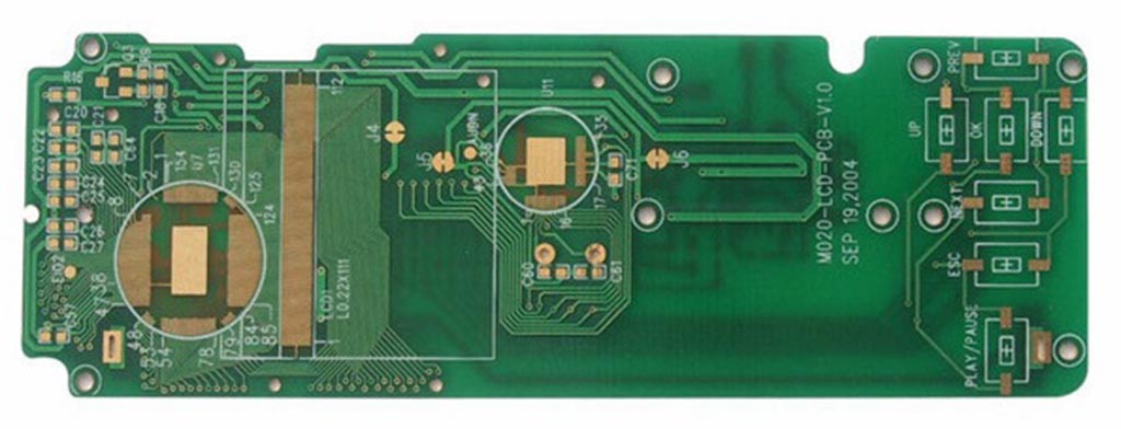
工藝分析 PCB板製造

(1) Use Laser photo plotters for drawing film to make wiring film, 阻焊膜, 生產過程中的印刷薄膜和其他必要薄膜.
貼膜過程中, 會有一些錯誤, 特別適用於特殊製版, 誤差會更大. 因此, 這些誤差的影響應在 PCB板製造 設計, 應進行適當的設計.
(2) Cutting of plates
The size of the board made of PCB板 at the factory is usually 1m*1m or 1m*1.2米. 根據生產需要, cut into different sizes of work pieces (work), 根據 PCB板設計 by yourself, 避免浪費和新增不必要的成本.
(3) Formation of inner circuit
Next, 形成內層的電路佈線. Paste a photosensitive dry film (dry film) on the double-sided copper plate as the inner layer, 然後粘貼用於製作內層佈線的薄膜, 暴露它, 然後執行開發過程, 僅在需要的地方保留接線. 該項目必須在雙方進行, through the etching ((Etching)) device, 去除不必要的銅箔.
(4) Oxidation treatment (blackening treatment)
Before being combined with the outer layer, 銅箔必須經過氧化,以形成細小的不均勻表面. 這是為了新增絕緣和粘合預浸料與內層之間的接觸面積,以提高粘合性. 現今, 為了减少環境污染, 已開發出氧化處理的替代品, 今天的 PCB板 自身接觸良好.
(5) Laminating treatment
After the oxidation treatment of the inner layer circuit, 塗抹半固化劑, 然後粘貼外層銅板. 在真空狀態下, 它由層壓機加熱和壓縮. 半固化劑起粘合和絕緣作用. 層壓後, 雙面銅板的外觀看起來一樣, 後續工程與雙面銅板相同.
(6) Opening
The CNC machine tool performs hole-opening operations.
(7) Remove residue
The heat generated during the opening of the hole will cause the filling to melt and adhere to the inner wall of the electroplated hole, 可通過化學物質去除,使內壁光滑,新增鍍銅的可靠性.
(8) Copper plating
The inner and outer layer connections need to be processed by copper plating. 第一, 化學鍍用於形成可流動電流的最小厚度. 其次, 為了達到設計要求的鍍層厚度, 進行電解電鍍. 因為外層銅箔也塗有銅, 外部痕迹的厚度是銅箔的厚度加上電鍍的厚度.
(9) Formation of outer circuit
As when forming the inner circuit, 粘貼光敏幹膜, 然後合上表面的接線膜, 和暴露. 曝光後, 只剩下佈線所需的地方, 並且兩面都經過處理. 然後, 通過蝕刻處理, 去除不必要的銅箔.
(10) Making solder mask
In order to form the pad, a solder mask (insulating layer) forming process is required, 它還可以保護銅箔和更好的絕緣. 該方法可以通過直接粘貼膠片, 或者先塗上樹脂,然後粘貼薄膜, 通過曝光和顯影去除不必要的區域.
(11) Surface treatment
In order to prevent oxidation of exposed copper parts without solder mask, 無鉛或無鉛鍍銅, 電解或非電解鍍金, 或表面處理需要水溶性化學清洗劑.
(12) Printing and printing
通常 the printing is white and the solder mask is green. 對於LED燈 PCB板, 為了達到更好的加强光源的效果, 印刷為黑色,焊接掩模為白色. 或者乾脆不用列印.
印刷對安裝和檢查電子元件的數量有很大的輔助意義. 但為了保密電路, 有時會犧牲列印.
(13) Shape processing
Process the shape of the PCB板 through a CNC punching machine or die
(14) Electrical testing engineering
Detect the open circuit and short circuit of the PCB板 through special electrical testing equipment
(15) Shipment
After checking the appearance and quantity of the PCB板, 可以發貨. Usually, 用脫氧資料包裝或直接運至安裝部件的工廠.