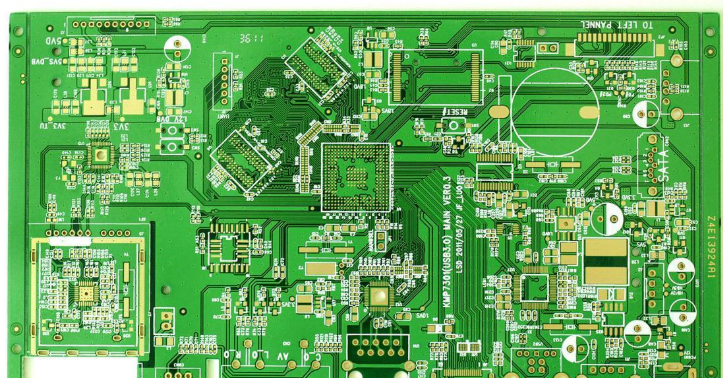
檢驗目的:驗證製造商生產的產品的焊點强度的可靠性 PCBA.
檢查方法和過程:
1、焊點目視檢查
(1) Use tools: X-Ray, 3-D microscope
(2) Main inspection, X射線主要檢查錫球焊點形狀, 短路, 取代, 空隙大小, 等. BGA的, LGA公司, QFN和其他部件; 3-D顯微鏡主要檢查漏鉛零件的焊點外觀, 和焊接角度. 等., 以及BGA部件週邊出現的錫球, 錫裂紋, 贓物, 等.
(3) Inspection frequency: X-Ray: For BGA and LGA products, 1每1K檢查一次面板. 引入了3維顯微鏡:用於BGA和LGA首件, 檢查四個側面和中心的5個顆粒外觀. Used when analyzing defective products
(4.) Inspection standard: Acceptance standard of Void size
IPC610D specification:
1. The bubble volume â ¤ 25% of the tin ball volume is the acceptable bubble acceptance standard:
2. The bubble volume 25% of the tin ball volume is unacceptable
Solder Balls displacement judgment standard:
1: Solder ball offset PADâ ¤25% is an acceptable level
2: Solder ball offset PAD 25% is unacceptable
Solder Balls Short Circuit Judgment Criteria: All short circuits are unacceptable even with tin
2. Solder joint strength inspection
(1) Tools used: push-pull machine and fixture
(2) Main inspection: resistance/電容/電感/標準操作程式, QFP和其他原始推拉力量測. 檢查頻率:新產品時檢查/新原件/new solder paste is introduced; when bad analysis
(3) Inspection standards: There are currently no inspection standards and empirical values in the industry, 除客戶要求外.

3. Dye test
(1) Tools used: dye, 真空泵, 烤箱, 3-D microscope
(2) Main inspection: Whether the tin balls of BGA parts are intact and whether there is tin cracking
(3) Inspection frequency: inspection at the time of new product/新原件/新錫膏介紹; at the time of failure analysis
(4) Inspection standards:
Crack (color display) is not allowed on PCBA 這還沒有做任何可靠性實驗.
PCBA 可靠性試驗後,焊點端層出現裂紋,25%可接受.
4. Section Inspection
(1) Use tools: grinding machine, 密封材料, 砂紙, polishing powder
(2) Main inspection: Cross-section observe the metallographic structure of the solder joints, 以及IMC的形成和焊點的結晶.
(3) Inspection frequency: inspection at the time of new product/新原件/new solder paste introduction; at the time of failure analysis
(4) Inspection standards:
Slice Solder Ball, QFP, SOP sample inspection:
1: Solder ball offset PADâ ¤25% is an acceptable level
2: Solder ball offset PAD 25% is unacceptable
3: Both short-circuit and empty welding at the solder joint ends are rejected.
4: Crack not allowed
5. Microstructure and element analysis
(1) Use tools: SEM electron microscope & EDX
(2) Main inspection: microstructure of solder joints, IMC厚度量測, and surface element structure analysis
(3) Inspection frequency: inspection at the time of new product/新原件/new solder paste introduction, and at the time of failure analysis
(4) Inspection standard: Solder Joint IMC thickness inspection:
PCBA 墊端:2-5um, Component Substrate 1-3um
EDX judgment: usually Solder Ball and element composition are: Sn/Ag公司/銅96.5%/3.0/0.5其中C和O的原子比在10%時正常. IMC層元素P的含量約為9-11%, 這很正常.