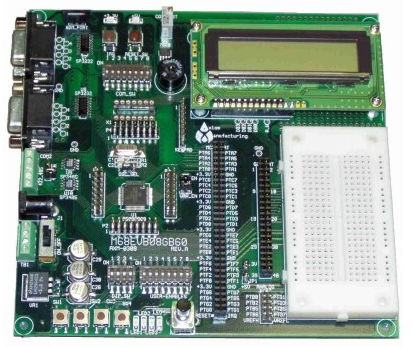
印刷電路板板 和集成電路不一樣? 有什麼區別?
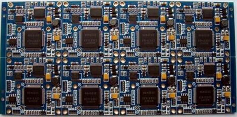
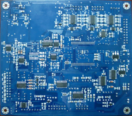
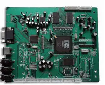
當前 電路板mainly consists of 這個 following:
1. Circuit and pattern (Pattern): The circuit is used as a tool for conduction between the originals. 在設計中, 此外,還將設計一個大的銅表面作為接地和電源層. 路線和圖紙同時繪製.
2 Dielectric layer (Dielectric): used to maintain the insulation between the circuit and each layer, 通常稱為基質.
3 Hole (Through hole / via): The through hole can make the lines of more than two levels connect to each other. 較大的通孔用作零件挿件. 此外, there are non-through holes (nPTH) usually used as Surface mount positioning, 用於裝配期間固定螺釘.
4 耐焊接 /阻焊膜:並非所有銅表面都需要鍍錫零件, so the non-tin area will be printed with a layer of 材料 that isolates the copper surface from eating tin (usually epoxy resin), 避免非鍍錫電路之間短路. 根據不同流程, 分為綠色油, 紅色油和藍色油.
5、絲印(圖例/標記/絲印):這是一種非必要的構圖。 主要功能是在電路板上標記各部件的名稱和位置框,便於組裝後的維護和識別。

6. 表面光潔度:因為銅表面在一般環境中容易氧化, it can not be tinned (poor solderability), 囙此,需要鍍錫的銅表面將受到保護. 保護方法包括HASL, ENIG公司, 化學銀, 浸入式錫, 和OSP. 每種方法都有其優缺點, 統稱為表面處理.
印刷電路板板 特徵
1、高密度:幾十年來,隨著集成電路集成度的提高和安裝科技的進步,印製板的高密度得以發展。
2. 高可靠性:通過一系列檢查, 試驗和老化試驗, the 印刷電路板 can work reliably for a long time (usually 20 years).
3、可設計性:對於印刷電路板效能(電力、物理、化學、機械等)要求,可以通過設計標準化、標準化等管道實現印製板設計,時間短、效率高。
4. 可製造性:利用現代管理可以進行標準化, scaled (quantitative), 自動化生產和其他生產,以確保產品品質的一致性.
5. 可測試性:一種相對完整的測試方法, 測試標準, 已建立各種測試設備和儀器,以檢測和評估 印刷電路板產品.
可裝配性: 印刷電路板 產品 are not only convenient for standardized assembly of various components, 而且還可以實現自動化和大規模生產. 同時, 印刷電路板 各種組件組裝件可以組裝成更大的零件和系統, 直至整機.