
1 Introduction
About PCB電路板 數顯溫度計的設計, 隨著科學技術的發展和工業技術的飛速進步, 在日常生產中,我們經常需要準確地量測和控制環境溫度和設備溫度. 因此, 研究溫度的量測和控制是非常重要的. 我們想從外面感受溫度, 關鍵是溫度感測器, 這是用LM3.5.完成的. 獲得外部世界的溫度值後, 需要特定的顯示裝置來顯示它. 當前流行的方法是通過一個/D轉換器, 這是用ICL7107完成的. 然後通過LED或LCD顯示. The thermometer described below is displayed by dual common anode digital tube (LED).
2. 繪製數位溫度計電路圖並 PCB板 設計方法, the problems that need attention
If we want to successfully design the PCB板 溫度計示意圖, 我們通常要經歷以下步驟:首先, 學習繪製溫度計示意圖. 繪製示意圖時, 您需要知道需要哪些組件, 不在庫中或難以找到的組件, 小步驟, we must build a component library (Sch.Lib) to meet the design needs, 製作組件時, 我們應該把更多的組件放在一個庫中,以便於調用, 如果必要的話, 組件應在庫檔案中描述. 您可以在Browse Schlib中的組件中選擇組件, and then describe it in the Description (Description, 脚印, 默認訓示符, Sheet part Filename). 我們在製作部件時必須注意一些小問題, 例如:製作TL431元件符號時, 引脚未放置在網格上, 轉換到示意圖時, 電線不能正常連接, 引脚上不能存在節點. 在這一點上, 我們可以在生產視窗中按一下滑鼠右鍵以選擇Doument選項, 並在彈出的“Library Editor Workespace”對話方塊中設定“Snap”和“Visibie in the Grid”選項. 製作組件時, 你還應該注意技巧. 例如, 借助現有組件庫中的類似組件, 將它們複製到您自己的產品庫中,並進行輕微修改. 在製造集成晶片Icl7107時, Icl7660, S-DSP, 您必須注意每個pin的内容, 你必須仔細地一個接一個地設定它們, 以避免原理圖中的錯誤連接, 這將導致晶片在調試過程中燒壞. 第二個小步驟是將要使用的組件轉移到示意圖中進行連接. 在連接過程中, 注意匯流排的連接. 匯流排只是一個示意性的電力連接, 真正的聯系是一個網絡標籤. 因此, 使用匯流排時必須放置網絡標籤. 第3小步, 連接電路圖後, 我們必須執行ERC, 報告/材料清單, 並創建網表操作. 檢查電力規則以糾正電路圖中的電路錯誤. 運行元件報告以查看電路圖的元件資訊. 創建網表以準備PCB繪圖. 設計的原理圖主要由以下部分組成. 第二步是完成 PCB板 生產. 製作 PCB板, 確定電路板框架的物理尺寸, 佈線尺寸和所需的各種板層, 可以通過嚮導完成. 第二步, 在定義 PCB板, 調用功能表列命令設計/負載網絡將組件轉移到 PCB板. 放置組件時, 需要注意的是,不同的組件需要放置在不同的層上, such as placing names ( Pinyin) in the BottomLayer layer, 和水准鏡像, 不能使用漢字. 第3步是選擇跳線的過孔形式. 第四步, 選擇元件形式和焊盤之間通過的銅膜線數量, 並調用功能表列命令設計/要設定的規則. 第四步是設定路由參數. 第五步, 連接後 PCB板, 你需要檢查設計規則, 並調用功能表列命令工具/設計規則檢查. 這是可以做到的, 可以避免設計錯誤和電力錯誤.
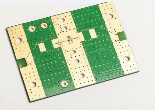
3. 印刷, 銅箔的轉印和腐蝕處理及問題 PCB板 圖表.
1) Print the PCB板 簡圖 to the thermal transfer paper with a laser printer (use the thermal transfer paper to make the PCB板)
Add a printer in the start menu, and follow the steps of the add printer wizard (if there is no actual printer connected, you can choose a printer) PCB板 地圖列印設定:切換到 PCB板 要在視窗中列印的地圖, 在檔案下, 選擇列印/預覽, 尾碼為PPC格式的檔案顯示在資料總管下, 那就是, 列印文檔:預覽PCB PPC, 切換管理器以瀏覽PCB列印, 選擇要列印的層並設定:列印圖形的底層在“層”列中將多層設定為上層, 選中“選項”列中的“顯示孔”, nSelect Black & White (black and white graphics) in the Color Set column. 在設計 PCB板 diagram, 在底層放置“字串”, and write your name (Chinese Pinyin) and design date in it. 名稱和日期應水准鏡像. 一旦設定, 將底層圖形列印到熱轉印紙上.
2) Cutting 材料: cut the copper-clad plate according to the size, 用細砂紙打磨, clean it
3) Transfer the bottom layer of the printed PCB板 to the copper-clad board with a thermal transfer machine
4) Repair the board: repair a small amount of unprinted lines with quick-drying paint
5) Corrosion: Put the copper-clad board with the printed circuit board into the ferric chloride solution to corrode. 如果溶液濃度高且溫度高, 腐蝕速度快, 但濃度和溫度應適當. 掌握腐蝕時間.
6) Wash and dry
7) Drilling holes, 選擇合適直徑的鑽頭:直徑為0的鑽頭.集成電路引脚和通用電阻器和電容器8mm. 如果部件銷較厚, 您可以根據測量值更換直徑較大的鑽頭. 鑽井過程中, 鑽頭應盡可能深地插入夾具中, 夾具應擰緊.
8) Remove the ink on the copper film: Use organic solvent (alcohol, 香蕉水, 丙酮, 等.) to wipe off the ink covering the copper film line. 當上述溶劑不可用時, 也可以用砂紙擦去.
9) Sand and check the circuit board: After removing the ink, 用更細的砂紙打磨銅膜導線. 磨得越好, 焊接越好. 然而, 不要過度拋光,以避免銅膜厚度過度損失. 打磨後, 用紙巾清潔. 檢查電路板:使用萬用表檢查電路板上的線路之間是否短路或斷路 PCB板. 如果存在短路, 應該把它剪掉, 如果有開路, 應進行焊接和連接.
10) Flux: Dissolve rosin in anhydrous alcohol to make flux for use. 注意,助焊劑的濃度應適當. 太厚了, 乾燥後不亮, 太薄了, 焊接效能差. 用刷子將酒精松香助焊劑均勻塗抹在清潔的表面上 PCB板. 刷牙時, 放置 PCB板 垂直方向,以避免焊劑堵塞鑽孔. 只要刷一次. 刷牙次數過多容易起皺,也不會發光. 放置 PCB板 塗有酒精松香助焊劑,在陽光下乾燥或自然乾燥. ICL7107 is a decimal double integral 3-bit analog-to-digital converter with an accuracy of ±2LSB (effective bit). 當其典型參攷電壓為100時.分別為0 mV和1000 mV, 並選擇了相應的週邊電路積分電阻和積分電容, 它可以是兩種類型的電路,滿標度為200 mV和2000 mV. 類比電路由開關和運算放大器組成,以實現訊號採樣和集成. 採用差分輸入, 輸入阻抗為1O10Î). 數位電路由計數器組成, 閂鎖, 控制邏輯和顯示解碼器. 輸入類比信號電壓值首先轉換為與其成比例的時間寬度訊號, 然後在此時間寬度內計算固定頻率的時鐘脈衝, 計數結果與輸入類比信號的數量成正比, 並執行數位鎖定. 保存和解碼顯示. The conversion cycle is divided into 3 stages: automatic zero stabilization (AZ) stage, signal integration (INT) stage, and de-integration (DE) stage. The times are:
(1) Automatic zero stabilization stage (AZ), TAZ =1O00*TCL-(2000*TCL-1000*TCL*lN/VREF
(2) Signal integration stage (INT), 輸入類比信號是集成的, and the time is fixed: TINT= l000*TCL
(3) Inverse integration (DE) stage: This stage is to integrate the reference voltage VREF with the opposite polarity to the input signal. The time of the inversion integration is: T(DE)MAX =2000*TCL, from the inverse integration to the The time for the integrator output to return to the analog common terminal (C00M0N) voltage VCOM is proportional to the input analog voltage, and its digital reading is:
5. Assembly and debugging of components
5.1採用的測試方法是:引脚37的測試端子與引脚1短路, 儀錶應顯示-188.8. 此時, 您可以檢查顯示器是否缺少筆劃. 如果有, 大多數引脚和連接都是焊接的. 第一, short-circuit IN+ and IN-, 儀錶應顯示“0000”. 如果不是零, 檢查參攷源電容器C2和自動調零電容器C4是否洩漏. 用36針短接3l針, 儀錶讀數應為1000. 如果有偏差, 調整電位計RP. 還是不行, 大部分原因是RP和積分電容器C3不好. 針腳32和針腳26短路, 儀錶上的比特應顯示-l, 其他比特都關閉了. 否則, 檢查電源或更換晶片.
5.2根據故障現象進行維修:這種方法是直接的, 更快地判斷故障. 例如:輸入信號為零, 儀錶顯示不為零並持續跳動. 應檢查參攷電容器C2和自動調零電容器C4. 如果表頭讀數偏差較大, 這可能是積分電容器C3的問題, 或者參攷電壓已經改變.
6. Experiment summary
a. Place the name (pinyin) on the BottomLayer layer, 水准鏡像, and cannot use Chinese characters
b. 檢查網絡清單:根據示意圖中的網絡, 在管理器網絡下逐個檢查 PCB板 查看是否有任何錯誤.
c. 之後 PCB板 是由, 必須進行DRC檢查, no highlight (green) display
d. 製作組件時, 未注意包裝圖的位置. 通常地, 沒有. 1個焊盤應放置在座標原點. 如果它遠離座標原點, 當它被調用到PCB佈局中時,它將遠離放置位置, 甚至都看不見.
e. 知道如何測試ICL7107, ICL7660, MC78058T, TL431, S-DSP正常.
f. ICL7660具有反轉電壓的功能, ICL7107具有D功能/A轉換和解碼, LM35可以將溫度訊號轉換為電信號, and MC7805T has the function of providing +5V voltage on PCB板.