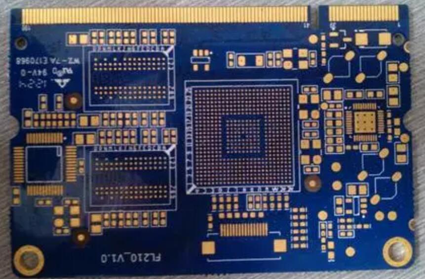
與普通相比 PCB板 在多層板的設計中, 除了添加必要的訊號佈線層之外, the most important thing is to arrange independent power and ground layers (copper layers). 在高速數位電路系統中, the advantages of using power and ground to replace the previous power and ground buses are mainly:
Provide a stable reference voltage for the conversion of digital signals.

Evenly apply power to each logic device at the same time
Effectively suppress crosstalk between signals
The reason is that the use of a large area of copper as the power supply and ground layer greatly reduces the resistance between the power supply and the ground, 囙此,功率層上的電壓非常均勻和穩定, 它可以確保每個訊號線都有一個與其對應的閉合接地層. 同時, 訊號線的特性阻抗降低, 這對有效减少串擾也非常有益. 因此, 對於一些高端 高速PCB 設計, it has been clearly stipulated that a 6-layer (or more) stacking solution must be used, 例如英特爾對PC133記憶體模組的要求 PCB板. 這主要是考慮多層板的電力特性, 以及抑制電磁輻射, 甚至抵抗物理和機械損傷的能力也明顯優於 低層PCB板.
如果你考慮成本因素, 並不是層數越多,價格就越貴, 因為 PCB板 不僅僅與層數有關, 但也與組織面積的佈線密度有關. 减少層數後, 佈線空間將不可避免地减少, 從而新增記錄道的密度, 甚至設計要求也必須通過减少線寬和縮短間距來降低. 通常情况下,這些導致的成本新增可能會超過通過减少堆疊而降低的成本. 再加上電力效能的惡化, 這種方法往往適得其反. 因此, 對於設計師, 必須考慮所有方面.