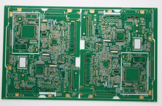
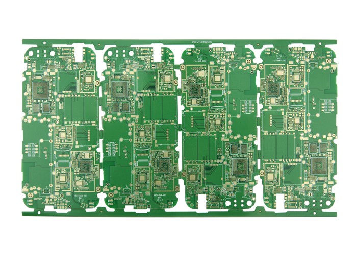
瞭解PCB板每一層的作用
就在上面, 我們介紹了 PCB板 有, 並簡要介紹了每個 電路板層. 今天,我們將更詳細地瞭解 PCB板. PCB電路板 一般分為六層, 具體為:機械層, 禁止佈線層, 阻焊層, 焊劑層, 絲網層和過孔層.

機械層
Protel 99 SE提供16個機械層, 通常用於設定電路板的外部尺寸, 數據標記, 對齊標記, 裝配說明和其他機械資訊. 該資訊因設計公司或 PCB製造商. 執行功能表命令設計|MechanicalLayer可以為電路板設定更多的機械層. 此外, 可以將mechanical層添加到其他層以一起輸出和顯示.
Prohibited wiring layer
Used to define the area where components and wiring can be effectively placed on the circuit board. 在此圖層上繪製一個閉合區域作為佈線的有效區域. 在此區域外無法進行自動佈局和佈線.
Solder mask
Apply a layer of paint, 如阻焊劑, 除襯墊外的所有零件,以防止這些零件上有錫. 焊接掩模用於在設計過程中匹配焊盤,並自動生成.
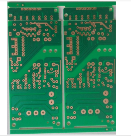
Soldering layer
The soldering layer is used for machine patching. 對應所有貼片組件的焊盤. 大小與頂部相同/底層. 用於打開模具漏錫.
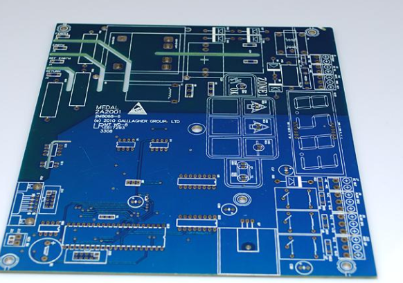
Silk screen
The silk screen layer is mainly used to place printed information, 例如組件輪廓和注釋, 各種注釋字元, 等. Protel 99 SE提供兩層絲印, 頂部覆蓋和底部覆蓋. 通常地, 各種各樣的標記字元都在絲網的頂層, 並且底部絲網層可以閉合.
Drilling layer
The drilling layer provides drilling information during the circuit board manufacturing process (such as pads and vias need to be drilled). Protel 99 SE提供兩個鑽孔層, Drillgride (drilling indication map) and Drill drawing (drilling drawing).
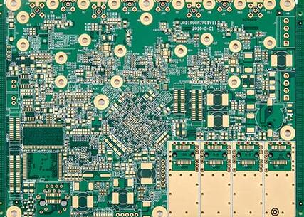
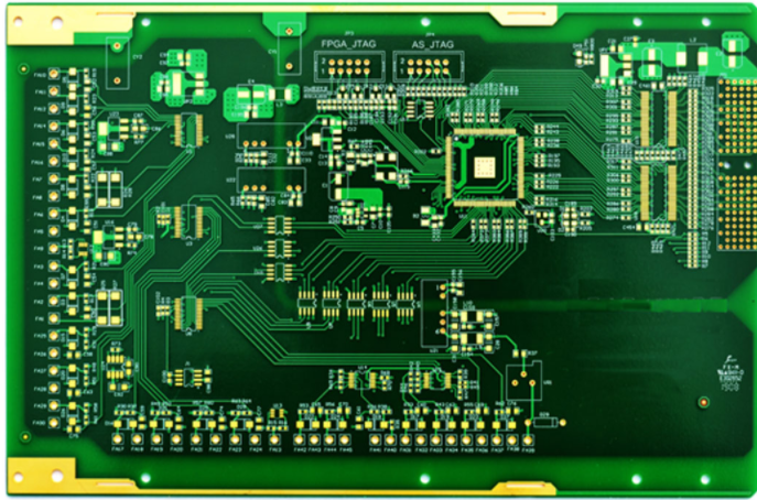
各層的作用 PCB板
雖然麻雀很小,但它的五個內臟都有PCB電路板,可以說執行了這樣一句老話。 PCB電路板的主要發展方向也是小型化和精密化。 囙此,對於每一層電路板,科技人員需要仔細選擇並仔細焊接它們,以便為主要製造商和個人提供更複雜的PCB電路板。