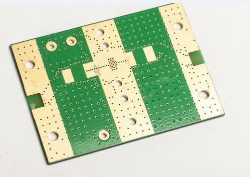

從電源佈局開始 PCB電路板, 本文介紹了PCB佈局方法, 優化電源模組效能的示例和科技. 規劃電源佈局時, 首先考慮的是兩個開關電流回路的物理回路面積. 雖然這些回路區域在電源模組中基本不可見, 當兩個回路延伸到模塊之外時,瞭解其各自的電流路徑仍然很重要. The current self-conducting input bypass capacitor (Cin1) passes through the high-side MOSFET during the continuous on-time of the MOSFET, reaches the internal inductor and the output bypass capacitor (CO1), 並返回到輸入旁路電容器. 在內部高側MOSFET的關閉時間和低側MOSFET的開啟時間期間形成. 存儲在內部電感器中的能量通過輸出旁路電容器和低側MOSFET流回GND. The region where the two loops do not overlap each other (including the boundary between the loops) is the high di/dt電流區域. The input bypass capacitor (Cin1) plays a key role in supplying high frequency current to the converter and returning it to its source path. The output bypass capacitor (Co1) does not carry as much AC current, 但它可以作為開關雜訊的高頻濾波器. 基於上述原因, 輸入和輸出電容器應盡可能靠近模塊上各自的VIN和VOUT引脚. 如圖2所示, 通過保持旁路電容器與其各自的VIN和VOUT引脚之間的軌跡盡可能短和寬,可以最小化這些連接的電感.

降低變壓器中的電感 PCB板 佈局有兩個主要好處. 通過促進Cin1和CO1之間的能量轉移來提高設備效能. 這將確保模塊具有良好的高頻旁路, 降低高電壓引起的感應電壓峰值/dt電流. 它還可以降低設備雜訊和電壓應力,以確保正常運行. 第二, 减少電磁干擾. 連接寄生電感較小的電容器將表現出對高頻的低阻抗特性, 從而减少傳導輻射. Ceramic capacitors (X7R or X5R) or other low ESR type capacitors are recommended. 只有當額外的電容器靠近GND和VIN端子時,添加更多的輸入電容器才會起作用. 功率模組的獨特設計固有地具有低輻射和傳導EMI, 並且遵循本文中提出的PCB佈局指南將產生更高的效能. 經常忽略回路電流的路徑規劃, 但它在優化電源設計中起著關鍵作用. 此外, 應盡可能縮短和加寬Cin1和CO1的接地軌跡, 並直接連接到外露的焊盤上, which is especially important for the input capacitor (Cin1) ground connection with high AC current. Ground pins (including exposed pads), 輸入和輸出電容器, 軟啟動電容器, 模塊中的迴響電阻應全部連接到PCB上的返回層. 該返回層可用作極低電感電流的返回路徑,也可用作下文討論的散熱器. The feedback resistor should also be placed as close as possible to the FB (feedback) pin of the module. 最大限度地减少該高阻抗節點處的潜在雜訊選取, 保持FB引脚和迴響電阻器中心抽頭之間的軌跡盡可能短至關重要. 可用的補償元件或前饋電容器應盡可能靠近上部迴響電阻器.
Thermal Design Recommendations
While the compact layout of the module provides electrical benefits, 這對熱設計有負面影響, 從較小的空間耗散等量的功率. 考慮到這一點, 功率模組封裝背面設計有一個大型外露焊盤,並進行電力接地. This pad helps provide very low thermal impedance from the internal MOSFET (which usually generates most of the heat) to the PCB. The thermal impedance (θJC) from the semiconductor junction to the outer package of these devices is 1.9°C/W. 而達到行業的JC值是理想的, low θJC values are meaningless when the thermal impedance (θCA) of the outer package to air is too great! 沒有到周圍空氣的低阻抗散熱路徑, the heat* cannot be dissipated on the exposed pad. 所以, 究竟是什麼决定了θCA值? 從暴露的焊盤到空氣的熱阻完全由PCB設計和相關散熱器控制. 現在快速瞭解如何在沒有散熱器的情况下進行簡單的PCB熱設計, 因為與從結到晶片墊的熱阻抗相比,結和外包裝頂部之間的熱阻抗相對較高, in this estimate from When considering the thermal resistance (θJT) from the junction to the surrounding air, 我們可以忽略ÎJA散熱路徑. 熱設計的第一步是確定要耗散的功率. The power dissipated by the module (PD) can be easily calculated using the efficiency graph (η) published in the datasheet. 然後,我們使用設計的兩個溫度約束, TAmbient和額定結溫, TJunction (125°C), 確定封裝在PCB上的模塊所需的熱阻. We use a simplified approximation of convective heat transfer from the surface of a PCB (with undamaged one-ounce copper heat sinks and numerous thermal vias on both the top and bottom layers) to determine the board area required for heat dissipation. The required PCB area approximation does not take into account the role of thermal vias that transfer heat from the top metal layer (where the package is connected to the PCB) to the bottom metal layer. 底層作為第二表面層,對流可以將熱量從板上轉移出去. 對於有效的電路板面積近似值, 使用至少8-10個熱過孔. 熱通孔的熱阻由以下方程值近似. 該近似值適用於直徑為12密耳和0的典型通孔.5盎司銅質側壁. 在外露襯墊下方的整個區域設計盡可能多的散熱孔, 並使這些散熱孔形成一個間距為1:1的陣列.5毫米. 電源模組為複雜的電源設計和與直流相關的典型PCB佈局提供了一種替代方案/直流變流器. 雖然佈局挑戰已經消除, 仍需進行一些工程工作,以優化具有良好旁路和熱穩定性的模塊效能 PCB板 設計.