快看! PCBA加工工藝
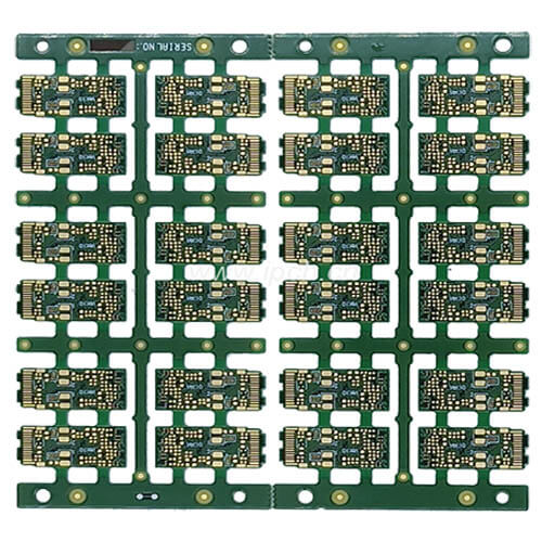
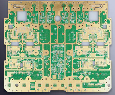
印刷電路板, 各種集成電路和電子元件是 PCBA生產 線. 這些原材料可以通過生產線準確地放置我們需要的集成電路和電子元件,並將它們焊接在 印刷電路板 成為電腦, 彩色電視, 這個 主電路板 通信設備的. 本文的主要內容是介紹 PCBA 過程ing 讀者流程, 讓您在荧幕前對 PCBA加工 過程, 讓我們看看!
The first step: solder paste printing
The squeegee advances 這個 solder paste along the surface of the template. 當焊膏到達範本的開口區域時, 刮板施加的向下壓力迫使焊膏穿過範本的開口區域,落在電路板上.

Step 2: Apply adhesive
Optional process. 為了防止波峰焊時的底面安裝組件或雙面回流焊時的底部大型集成電路組件熔化和掉落, the 雙面組裝電路板需要粘到組件上.
第3步:零部件放置
此過程是使用自動放置機從進料器中拾取表面安裝組件,並將其準確安裝到印刷電路板上。
Step 4: Inspection before and after welding
Before the components are reflow soldered, 必須仔細檢查組件是否安裝良好,位置是否偏移.
Step 5: Reflow soldering
After the component is placed on the solder, 焊盤上的焊料通過熱對流科技的流動焊接過程熔化,在元件引線和焊盤之間形成機械和電力互連.
The sixth step: component insertion
For through-hole plug-in components and surface-mount components that cannot be mounted on certain machines, 如插入式電解電容器, 連接器, 按鈕開關, and metal terminal electrode components (MELF), 手動插入或使用自動插入設備插入組件.
Step 7: Wave soldering
Wave soldering is mainly used to solder through-hole plug-in components.
Step 8: Cleaning
Step 9: Repair
This is an off-line process whose purpose is to economically repair defective solder joints or replace defective components.
Step 10: Electrical test
Electrical testing mainly includes online testing and functional testing.
Step 11: Quality Management
Quality management includes quality control in the production line and product quality assurance before delivery to customers.
The twelfth step: packaging and sampling inspection
The last step is to pack the components and conduct sampling inspections after packaging to again ensure the high quality of the products that will be delivered to customers.
主機板是科技電子產品的核心部件, 所有功能的正常運行都與之密切相關. 這只是對 PCBA加工 process. 如果要細分和擴展, 過程並不是那麼簡單. 我希望這篇文章或多或少能幫助您理解PCBA流程, 它還可以揭開更多關於PCBA的謎團.