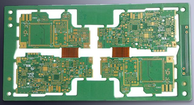
PCB Design content and manufacturability Design Implementation Procedure PCB Planning Color comprend la sélection des données de l'équipement du substrat et des composants, la planification des circuits imprimés, la planification des processus (fabricabilité), la conception de la fiabilité SMT et la réduction des coûts de production. La subdivision est illustrée ci - dessous. Les procédures de planification et de mise en œuvre de la fabricabilité des plaques imprimées SMT sont les suivantes 1. Confirmation de la fonctionnalité, des indicateurs de performance et des objectifs généraux de la taille globale de l'électronique Ce sont les facteurs qui ont été pris en compte lors du premier test de la planification de la fabricabilité des cartes imprimées SMT. Effectuer le principe électrique et la planification de la structure mécanique, déterminer la taille et la forme structurelle du PCB en fonction de la structure complète de la machine

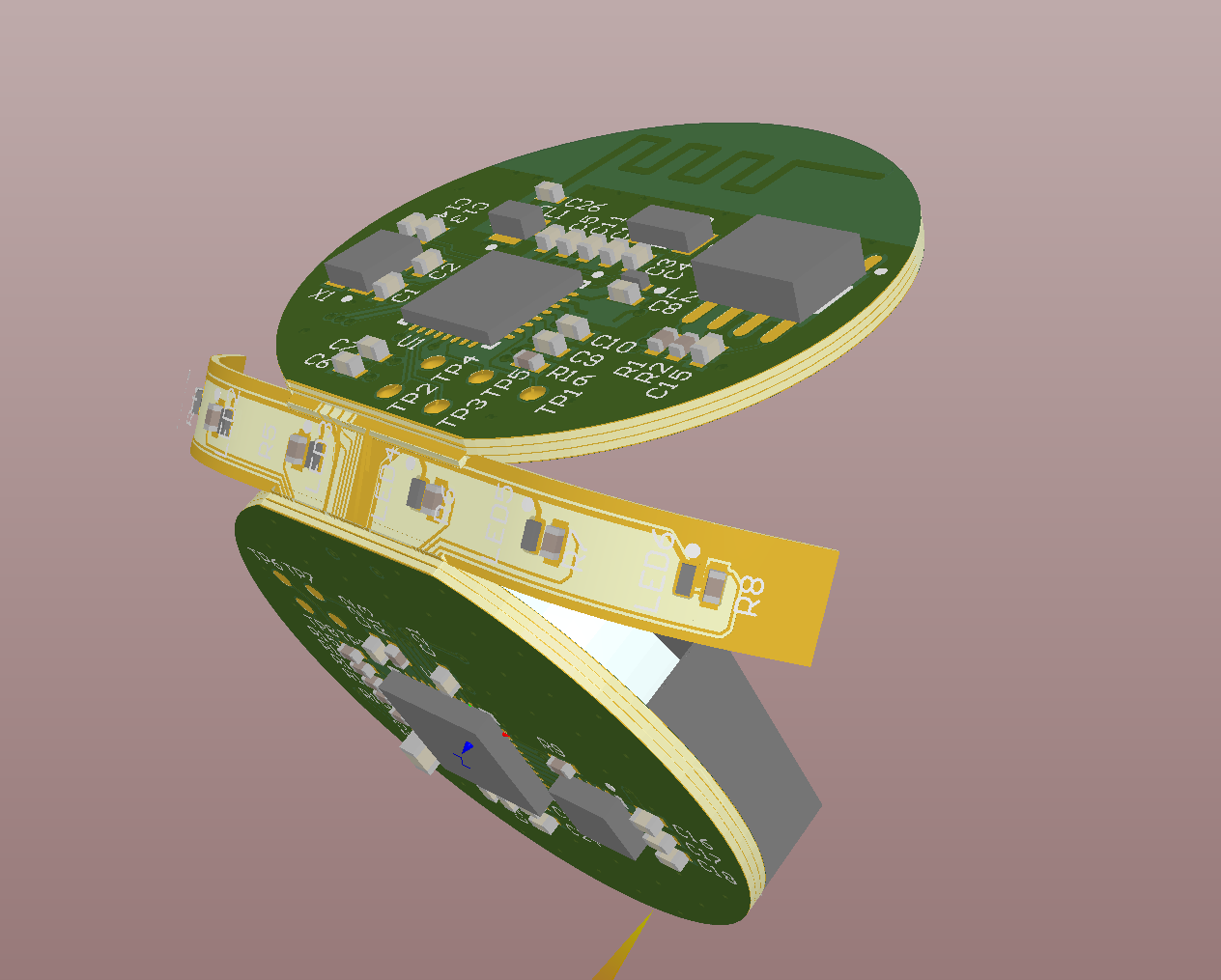
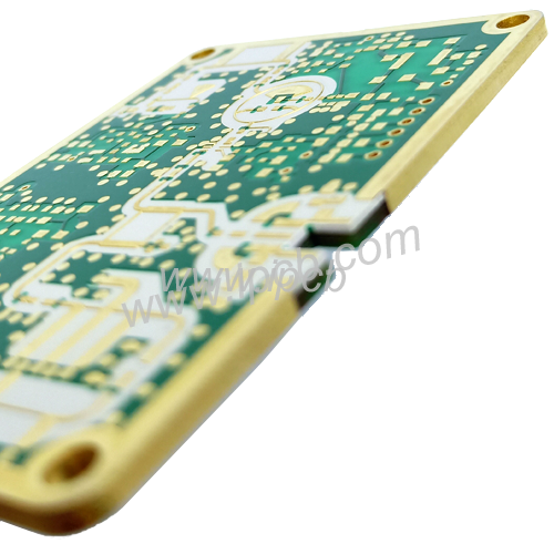
Draw the outline planning process layout of the SMT printed board, as shown in Figure 5-12. When confirming the size and structure of the PCB, it is necessary to consider the structure of the electronic product, but also to test the clamping edges of the printer and placement machine, mark the length, width, and thickness of the PCB, and set aside the position and size of the structural component mounting holes. The clamping edge cannot be placed on the scale of the component, the edge scale of the pad, etc., so that the circuit planner can carry out wiring and component layout planning within a useful range.3. Appearance assembly method and process planning Appearance assembly method and process planning are reasonable and fragrant, which directly affect assembly quality, production efficiency and production cost.The assembly class picture and process flow of SMA are in principle specified by PCB planning, because different assembly methods have different requirements for pad planning and component column direction. A good plan should be Direction of PCB rotation during soldering are marked on the outside of the PCB, and the production process and operation direction specified in the planning should be followed completely.4. The function, performance index and product level of the root product select PCB materials and electronic components(1)Select PCB data (2) Select elementary equipment According to the circuit requirements of the specific product, as well as the PCB size, assembly density, assembly method, product extension and investmentCost to choose yuan equipment.1. Selection of SMC-- Pay attention to the size and accuracy of the scale, and test the history to satisfy the function of the placement machine.-- Heliu electrolytic capacitor main ammonia is used in occasions with large capacitance-- Film capacitors are used in occasions with high demand for heat.-- Mica capacitors are used in high-value mobile communications.-- The wave soldering process must select three-layer metal electrode solder end structure chip components.2. SMD selection.--Small outline package transistor: SO123 is the most commonly used triode package, SOT143 is used for radio frequency.-- SOP, SOJ: It is the reduced type of DIP, similar to the function of DIP.-- QFP: Occupies a large area, the lead is easy to deform, easy to lose coplanarity; but the flexibility of the lead can help release the stress and improve the generalThe reliability of solder joints. The minimum distance between the QFP pins is 0.3mm, and the current 0.5mm distance from this application is 0.3mm, 0.4mm'S QFP is gradually replaced by BGA. When selecting, pay attention to whether the precision of the placement machine meets the requirements.--PLCC: It occupies a small area and the pins are not easy to deform, but it is inconvenient to detect.--O LCCC: The price is expensive, and it is mainly used for high-reliability and military products. CET problems between loyalty equipment and circuit boards should be tested.--BGA, CSP: suitable for high IO circuits.3. Selection of chip electromechanical componentsPiece electromechanical components are mainly used in high-density, small, and light-weight electronic products.4. The selection of THC (instrument element equipment) At present, the country has higher and higher requirements for environmental protection and greater efforts in link governance. This is a challenge for PCB factories, but it is also an opportunity at the same time. If PCB factories are determined to solve the problem of environmental pollution, then FPC flexible circuit board products can be at the forefront of the market, and PCB factories can get opportunities for further development.