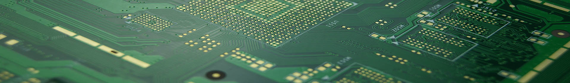
우리는 모두 PCB 보드가 완벽하게 전기를 전도하고 안정되기를 바라지만, 실제 상황은 그렇지 않다. 현실 세계는 완벽한 도체와 절연체로 이루어져 있지 않다. 그것들은 진공으로 둘러싸여 있고, 전장은 현실 시스템의 도체와 안감과 상호 작용한다.IC를 설계하든 PCB를 설계하든 불완전한 전자 제품의 중요한 영향인 전기 마이그레이션을 고려해야 한다.전기 마이그레이션이란 무엇이며 왜 발생합니까?더 중요한 것은 어떻게 예방할 것인가?간단한 PCB 및 IC 전기 마이그레이션 분석이러한 장치가 서로 다른 조건에서 단락과 개로를 방지하는 것이 목적이다.이를 위해 일부 업계 표준을 제정했다.이러한 표준과 마이그레이션으로 인해 새로운 장치가 고장나는 방법에 대해 알아야 합니다.
Electromigration in electrons
As more components are stacked in a smaller space, the electric field between two conductors with a specified potential difference becomes larger. This leads to some safety problems in high-voltage electronic equipment, especially electrostatic discharge (ESD). The high electric field between two conductors separated by air will cause the air to undergo dielectric breakdown, thereby generating an arc and a current pulse in the surrounding circuit. To prevent these discharges in PCB boards or other equipment, conductors need to be separated by a certain spacing, which depends on the potential difference between the conductors. The above gap distance is important for safety and preventing equipment failure, but the distance across the substrate is also important. Another point to consider is the distance between conductors across the dielectric. In PCB, this is called creepage distance. When the distance between conductors is small, the electric field may be large, resulting in electromigration. When the current density in a conductor is large (in IC), or when the electric field between two conductors is large (in PCB), the mechanism of driving electromigration can be described as exponential growth. To prevent electromigration, you can use three levers to pull in your design:
PCB 보드에서 도체 사이의 간격을 늘립니다.PCB 보드에서 도체 사이의 전압을 낮춥니다.낮은 전류(IC에서)로 장치를 조작합니다.
Electromigration in IC: open circuit and short circuit
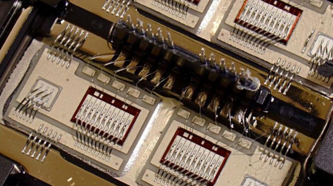
IC 상호 연결에서 주요 힘은 두 도체 사이의 전장과 그 후의 이온화가 아니다.반면 고체 전기 이동은 고전류 밀도에서 전자 동량 이동 (산란) 으로 인해 금속이 전도성 경로를 따라 이동하게 됩니다 (이 경우 금속 상호 연결 자체).이동 속도는 상호 연결 온도가 높아짐에 따라 증가합니다.구리 전기 이동에 관련된 힘은 다음과 같다.풍력이란 격자 속의 금속 원자로부터 전자가 산란되어 금속 이온에 가해지는 힘을 말한다.이런 중복된 이온화와 동량은 자유금속 이온으로 옮겨져 양극으로 확산된다.이러한 마이그레이션 프로세스에는 활성화 기능이 있습니다.금속 원자로 전이된 에너지가 아레니우스 활성화 과정을 넘어서면 정향 확산이 시작되는데, 이는 농도 경도(피크의 법칙)의 지도 아래 이뤄진다.금속이 도체 표면으로 당겨지면 두 도체를 브리지할 수 있는 구조를 만들어 합선을 초래하기 시작한다.또한 서로 연결된 양극 측면의 금속을 소진하여 길을 열 수 있습니다.다음 SEM 이미지는 두 컨덕터 간 확장 전기 마이그레이션의 결과를 보여줍니다.금속이 표면을 따라 이동하면 간격이 남거나 (열림) 인접한 도체에 연결되는 웨이퍼 (합선) 가 생성됩니다.구멍이 뚫리는 극단적인 상황에서 전기 마이그레이션은 커버 계층 아래의 도체까지 소진할 수 있다.
Electromigration in PCB: dendritic growth
Similar effects occur in PCB boards, resulting in two possible forms of electromigration:
As described above, electromigration along the surface, the formation of semiconductor salts, leads to the electrochemical growth of dendritic structures. These effects are controlled by different physical processes. The current density between the two conductors may be low because the size of the metal traces is very large compared to the cross section of the IC interconnect. In this case, migration will occur at high current density, resulting in the growth of the same type of stubs over time. On the surface layer, oxidation may subsequently occur as the conductor is exposed to air. In the second case, electromigration is an electrolytic process. This field drives electrochemical reactions in the presence of water and salt. Electrolytic electromigration requires water on the surface and high direct current between the two conductors, which will drive the electrochemical reaction and the growth of dendritic structures. The migrated metal ions are dissolved in the aqueous solution and diffused over the entire insulating substrate. Increasing the distance between adjacent conductors reduces the electric field between them, thereby suppressing the reaction of driving electrolytic electromigration. Electromigration analysis in the new layout needs to check the design to ensure that the trace gap does not violate design rules or industry standards. If you can use some basic PCB board or IC layout tools, you can check the layout against these rules and find any violations. With the shrinking of IC and
PCB board, electromigration analysis will only become more and more important to ensure reliability.