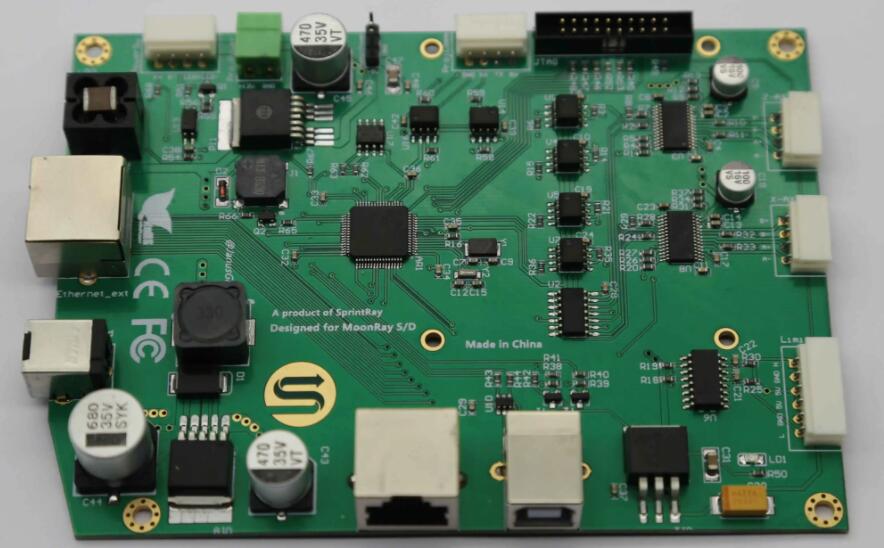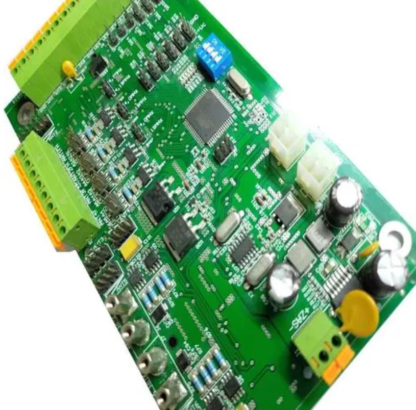

The reliability of printed circuit board assemblies (PCBAs) is paramount.
Testing During PCB Manufacturing
Our commitment to quality begins at the very foundation: the PCB manufacturing process. We employ stringent testing procedures to guarantee the integrity of the bare boards. This includes:
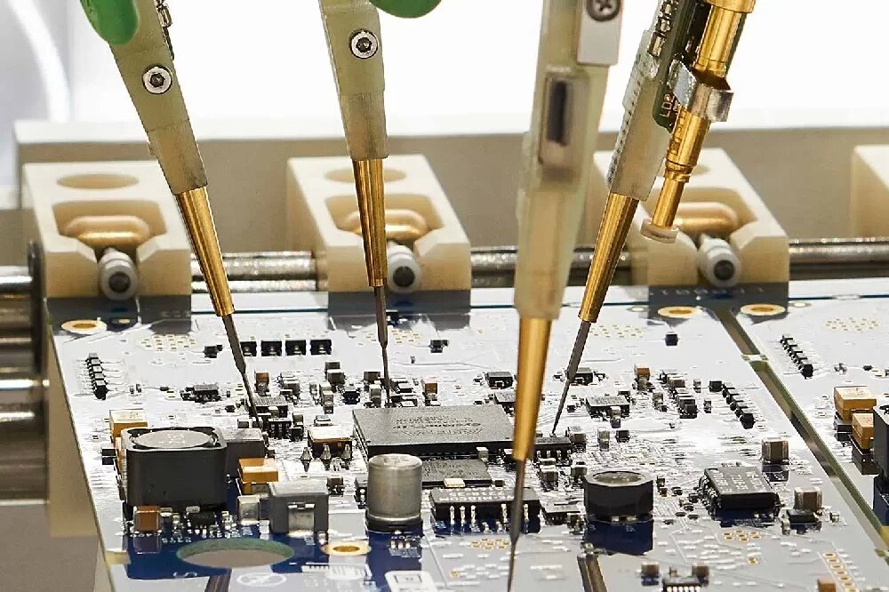
Electrical Testing (E-Testing): Utilizing flying probe or bed-of-nails testers, we verify the continuity and isolation of the PCB traces, identifying shorts and opens before assembly.
Automated Optical Inspection (AOI): This automated process detects visual defects such as scratches, voids, and misalignments in the PCB layers.
Impedance Control Testing: For high-frequency applications, we meticulously measure and control the impedance of critical traces to ensure signal integrity.
Micro-sectioning: This destructive testing technique allows us to examine the cross-section of the PCB to assess the quality of plating, drilling, and layer adhesion.
By addressing potential issues early in the manufacturing process, we minimize downstream defects and optimize the overall yield.

The Assembly and Soldering Phase: Validating Component Placement and Connections
The PCBA assembly and soldering stage introduces new complexities that necessitate comprehensive testing. Our services encompass:
AOI (Post-Reflow): After the reflow soldering process, AOI is employed again to verify component placement, solder joint quality, and identify potential defects like solder bridges, insufficient solder, and tombstoning.
X-Ray Inspection (AXI): For complex assemblies, particularly those with Ball Grid Array (BGA) packages, AXI provides non-destructive inspection of solder joints hidden beneath components.
In-Circuit Testing (ICT): ICT utilizes bed-of-nails fixtures to electrically test individual components and circuits on the assembled board, identifying functional defects and component value deviations.
Functional Testing (FCT): This crucial step simulates the real-world operating conditions of the PCBA, verifying its functionality and performance against specified parameters.

ODM: Engineering Support and Product Development with Integrated Testing
Our ODM services extend beyond manufacturing and assembly, encompassing engineering support and product development. This integrated approach allows us to incorporate testing considerations from the initial design phase. We provide:
Design for Testability (DFT): We collaborate with clients to optimize their designs for ease of testing, ensuring that critical test points are accessible and that test coverage is maximized.
Test Fixture and Software Development: Our engineering team develops custom test fixtures and software to meet the specific testing requirements of each project.
Reliability Testing: We conduct environmental stress testing, such as temperature cycling and vibration testing, to assess the long-term reliability of the PCBA.
Performance Characterization: We perform detailed performance characterization to ensure that the PCBA meets all specified performance requirements.

The Value of an Integrated Approach
By offering a comprehensive suite of services, from PCB manufacturing to ODM, we provide our clients with a streamlined and efficient solution for their PCBA needs. Our integrated approach offers several key advantages:
Reduced Lead Times: By consolidating all stages of the process under one roof, we minimize lead times and accelerate time-to-market.
Improved Quality Control: Our integrated quality management system ensures consistent quality throughout the entire process.
Cost Savings: By identifying and addressing potential issues early on, we minimize rework and reduce overall costs.
Enhanced Communication: Our dedicated project management team provides a single point of contact, ensuring clear communication and efficient project execution.
In conclusion, our commitment to rigorous PCBA testing, combined with our comprehensive service offerings, ensures that our clients receive high-quality, reliable products that meet their specific requirements. From the initial PCB manufacturing to the final ODM stage, we are dedicated to delivering excellence.