pcb impedance calculator is usually used in the design of Multilayer PCB, high-frequency PCB, and antenna PCB. We need to perform PCB impedance calculator and PCB impedance control in these high-frequency PCB signals to ensure the stability of PCB and the pass rate of various index tests.
With the development of science and technology, especially with the advancement of the materials of integrated circuits, the operation speed has been significantly improved, and the integrated circuit has become high density, small size, and single part. All of these have led to the high-frequency response of today's and future printed circuit boards and the use of high-speed digital circuits. That is, the impedance, low distortion, low interference and low crosstalk of the line must be controlled, and EMI must be eliminated. Impedance design is becoming more and more important in PCB design. The engineer of IPCB is the front-end Department of PCB manufacturing, responsible for the simulation of impedance and the design of impedance bars. Customers are increasingly demanding impedance control, and the number of impedance control is also more. How to design impedance quickly and accurately is a very important issue for pre-production CAM engineers.
What is pcb impedance calculator control in PCB?
1. Introduction of PCB impedance control concept
In order to distinguish the resistance of direct current (DC), the resistance encountered by the alternating current is called impedance (Z0), including resistance (R), inductive reactance (XC), and capacitive reactance (XL).
PCB characteristic impedance is also called "characteristic impedance". It refers to the resistance of PCB high-frequency signal or electromagnetic wave in the transmission signal line (i.e. the copper wire of PCB made by us) at a certain frequency relative to a certain reference layer (i.e. shielding layer, projection layer, or reference layer), which is called characteristic impedance in the process of propagation. It is actually the sum of a vector of resistance, inductance, capacitance, etc.

2. Significance of controlling pcb impedance calculator
PCB not only plays the role of current conduction in electronic products but also plays the role of signal transmission.
High frequency and high-speed PCB of electronic products require that the circuit performance provided by PCB must ensure that the signal does not reflect in the transmission process and keep the signal intact and undistorted.
PCB characteristic impedance is the core to solving the problem of signal integrity.
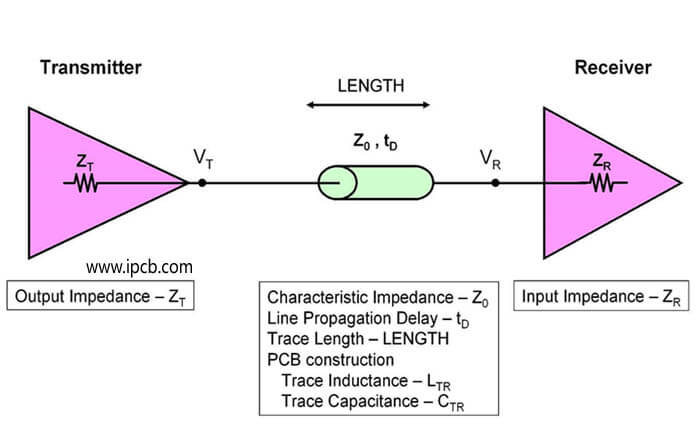
When electronic equipment (such as computer, communication switch, etc.) is operated, the signal sent by driver must reach the receiver through PCB signal line. In order to ensure signal integrity, the characteristic impedance (Z0) of PCB signal line must match the "electronic impedance" of head and tail components.
When the transmission line is more than 1 / 3 rise time, the signal will reflect, so PCB characteristic impedance must be considered.
3. Factors affecting pcb impedance calculator, the characteristic impedance of PCB trace.
Dielectric constant of PCB is inversely proportional to PCB characteristic impedance (ER)
The dielectric thickness between PCB circuit layer and ground plane (or outer layer) is directly proportional to the characteristic impedance value (H)
PCB impedance line bottom width (lower W1); line surface (upper W2) width, inversely proportional to the characteristic impedance
PCB copper thickness is inversely proportional to PCB characteristic impedance (T)
The distance between adjacent lines of PCB is directly proportional to the characteristic impedance value (differential impedance) (s)
The thickness of PCB substrate solder mask is inversely proportional to the impedance value (c)
4. Process factors affecting PCB impedance
Because of etching, when the thickness of copper is more than 2oz, the impedance of PCB can not be controlled.
In the design, there is no copper and wire layer blank, which needs to be filled with curing sheet during production. When calculating the impedance, the thickness of the medium provided by the plate supplier can not be directly replaced, but the thickness of the blank space filled by the curing sheet needs to be subtracted. This is one of the main reasons for the inconsistency between the impedance calculated by ourselves and the results of the manufacturer.
The calculation of impedance PCB is relatively cumbersome, but we can sum up some experience values to help improve the calculation efficiency. For the commonly used FR4, 50ohm microstrip line, the linewidth is generally equal to twice the thickness of the medium; for the 50ohm stripline, the linewidth is equal to half of the total thickness of the medium between the two planes. This can help us quickly lock the linewidth range. Note that the calculated linewidth is smaller than this value.
In addition to improving the calculation efficiency, we also need to improve the calculation accuracy. Do you often encounter the inconsistency between the PCB impedance calculated by yourself and the PCB Factory? Some people will say that this has nothing to do with it. Let the PCB Factory adjust it directly. But will there be PCB Factory can not adjust, let you relax PCB impedance control? To do a good job in the product or everything in their own control is better.

How do we control PCB impedance in design?
1. Use the experience value to record the impedance line that has been done before, for example, the line width of PCB and the thickness of the board, and apply it directly in the next use.
2. Firstly, according to the conventional design, highlight the lines that need to be impedance in PCB, and then give the screenshot to the PCB Factory. If the PCB Factory wants to control it, the PCB Factory will modify the data according to the PCB impedance we require, such as adjusting the PCB line width and line spacing to achieve the required impedance.
3. At the beginning of the design: according to the lamination parameters of PCB and the relevant data (PCB board, dielectric constant, green oil, PP thickness, etc.) provided by the PCB manufacturer, we calculated the impedance with si9000 software, and then used the calculated parameters to trace the impedance line, and finally obtained the PCB data to At the same time, the PCB factory needs the PCB Factory to control the impedance of PCB. The advantage of this is that in general, the PCB Factory will not move our data, and it is also a very small adjustment.
As you can see from the above,
Points 1 and 2 are not safe. In point 1, if the stack parameters of PCB are changed, then the impedance of PCB will also change. I don't know if there is a mistake on the day of continuous application,
2. It's OK to click the screenshots to be controlled by the PCB Factory. However, engineers from the PCB Factory often call to say that your PCB impedance can't be done. The reason is that the difference between the line width and line distance of the PCB designed by you is too big, and there is not enough space on the PCB to widen the line width and line distance.
Obviously, the third scheme is the safest, and the PCB Factory will not be able to control the impedance of PCB.

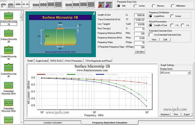
The most commonly used impedance calculation tool in our industry is the Si8000 Field Solver provided by polar company. Si8000 Field Solver is a new boundary element method field effect solution calculator software, which is based on the easy-to-use user interface of the early polar impedance design system we are familiar with. The software contains various impedance modules. The personnel can calculate the impedance results by selecting a specific module and inputting relevant data such as line width, line distance, dielectric thickness, copper thickness, er value and so on. The number of impedance control of a PCB is as few as 4 or 5 groups and as many as dozens of groups. The control linewidth, dielectric thickness and copper thickness of each group are different. If you check the data one by one and then manually enter the relevant parameters for calculation, it is very time-consuming and error prone.
Opal's inplan software can automatically design PCB impedance, greatly improving the pre manufacturing efficiency. The inplan system of Orbotech can be connected to si8000 and automatically calculate the impedance based on the establishment of the following database: first, establish a complete material warehouse in inplan and classify it according to different PCB manufacturers and models. Build in the data of pressing thickness, substrate copper thickness, PP glue content, etc. obtained according to the actual process parameters in the PCB Factory.
Then, establish rules for calculating impedance in inplan, such as green oil thickness and undercut value, and set rules according to different copper thickness, impedance module or inner and outer layers. The dielectric constant is written into the formula mainly according to the type of material and different impedance modules. Impedance value and impedance linewidth tolerance are also written into the rule through inplan rule. When calculating the impedance, inplan automatically brings out the relevant impedance influence parameter values according to the rules to calculate the optimized impedance results. And no matter how many impedance groups there are, all the results can be obtained in a few seconds by clicking a button.
If the customer does not design the PCB impedance strip by himself, we need to design the PCB impedance strip by ourselves and put it on the board edge or broken edge (generally, the placement of the impedance strip on the broken edge requires the consent of the customer). The circuit board manufacturer designs a PCB impedance strip that meets all the characteristics and parameters of the customer's PCB impedance control at the edge of the circuit board. By testing the PCB impedance value of the impedance strip, it reflects that the circuit board impedance meets the customer's requirements. In order to correctly test the impedance value in the board, the key lies in the design of the impedance strip.
The competition of PCB is becoming more and more fierce, the delivery time of PCB samples is becoming shorter and shorter, and PCB impedance design accounts for a large proportion in the work before PCB manufacturing. How to shorten the PCB impedance manufacturing time and make impedance matching to meet customer requirements is a problem that must be considered in the work before PCB manufacturing.
how to specify PCB impedance? You can also use this impedance calculator for PCB to calculate PCB impedance.
This is the PCB impedance calculator of Rogers company. Download PCB impedance calculator
The PCB impedance calculator method of IPCB company is: MI engineer fills in the impedance attachment table according to the calculated impedance results, such as impedance value, reference layer, control linewidth, test hole, Reference layer properties (positive and negative pieces), etc. then, cam engineers manually make impedance strips according to the impedance form provided by Mi, or input relevant impedance data through script, and run impedance strips by program. Generally, for a PCB impedance value, we design a PCB impedance strip and make a pcb impedance calculator.