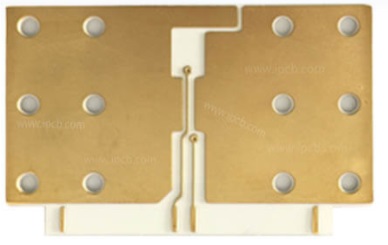

What is a glass substrate?
The chip substrate is used to fix the cut chips (Die) of the wafer, and is the protagonist of the final step of packaging. The more chips fixed on the substrate, the more transistors the entire chip has. Since the 1970s, chip substrate materials have undergone two iterations. At the beginning, chips were fixed using lead frames, and in the 1990s, ceramic substrates replaced lead frames. Nowadays, organic material substrates are the most common.
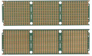
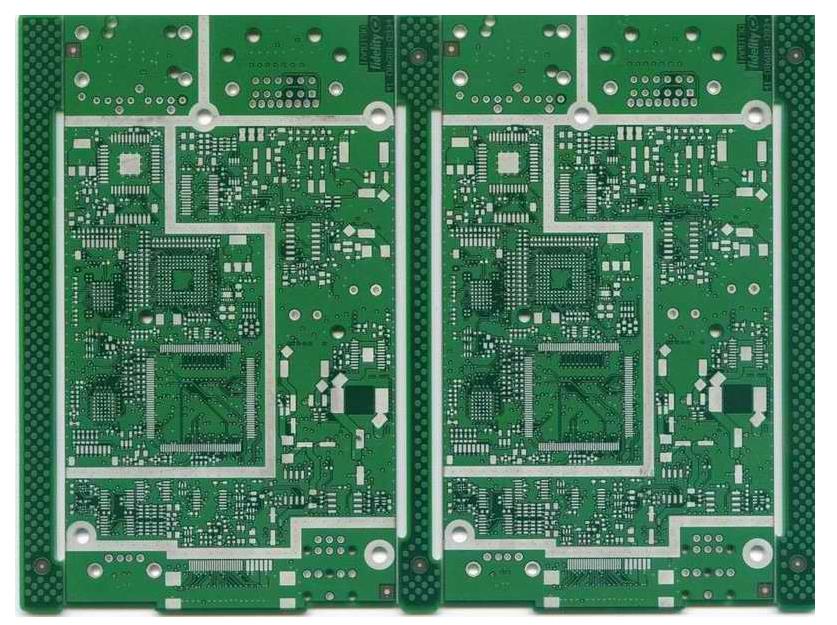
A standard circuit board is essentially made by laminating materials similar to PCBs with glass woven laminates. Organic material substrates have low processing difficulty and can also transmit high-speed signals, and have always been regarded as leaders in the field of chips. However, organic material substrates also have some drawbacks, such as a large difference in thermal expansion coefficient between them and the chip. At high temperatures, the connection between the chip and the substrate is easily broken, and the chip is burned out. It is necessary to carefully control the temperature of the chip through thermal throttling, which means that the chip can only maintain its highest performance for a limited time and then slow down to reduce the temperature. Therefore, the size of standard circuit substrates is greatly limited, and the material selection of the substrate is crucial to accommodate more transistors within the limited size.
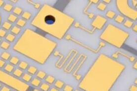
Glass substrate have excellent mechanical, physical, and optical properties, enabling the construction of higher performance multi chip SiPs with 50% more Die placed on the chip. In contrast, glass substrates have unique properties such as ultra-low flatness (extremely flat), better thermal stability, and mechanical stability. Due to the extremely flat glass material, it can improve the focusing depth of lithography. Under the same area, the number of openings is much larger than on organic materials. The spacing between glass through holes (TGVs) can be less than 100 microns, which can directly increase the interconnect density between chips by 10 times. In addition, the thermal expansion coefficient of glass substrates is closer to that of chips, and higher temperature tolerance can reduce deformation by 50%, which can reduce the risk of fracture and increase the reliability of chips. These advantages make glass substrates an ideal choice for the next generation of high-density packaging.
Compared to traditional standard circuit substrates, the thickness of glass core substrates can be reduced by about half. Glass substrate not only have lower power consumption, but also faster signal transmission speed, which is expected to bring speed and power advantages to large power consuming chips in servers and material centers. Glass through holes are now being successfully applied to glass substrates. Compared to the past, the new generation of processors will achieve more components in a smaller volume, thereby improving the compactness and performance of the device.
The fragility of glass substrate, lack of adhesion with metal wires, and uniformity of through-hole filling also pose significant challenges to the manufacturing process. Choosing the appropriate glass substrate material and ensuring its compatibility with chip materials is a challenge, which involves matching the material's thermal expansion coefficient, mechanical properties, dielectric properties, and other aspects. The connection technology on glass substrates requires high reliability and stability to ensure the quality of the connection between the chip and external circuits. Compared with traditional plastic packaging, the manufacturing cost of glass substrate packaging may be higher, and how to ensure consistent quality and performance in large-scale production is also a problem that needs to be solved.
The characteristics of glass substrates are very suitable for Chiplets, as the design of small chips imposes new requirements on the signal transmission rate, power supply capability, design, and stability of the substrate. After switching to glass substrates, these requirements can be met.
Compared with silicon, the high transparency and different reflection coefficients of glass also pose difficulties for detection and measurement. Many measurement techniques suitable for opaque or semi transparent materials are not very effective on glass, which may result in signal distortion or loss, affecting measurement accuracy.
Although there are still many challenges and a lack of reliability data, its unparalleled flatness and thermal performance provide the foundation for the next generation of compact high-performance packaging, making the potential of glass substrates as an important technology for the next generation of chips cannot be ignored. Replacing standard circuit board with glass materials seems to be becoming an industry consensus, or at least a very important technological path in the future.
Glass substrate technology is applied in chip development to provide better heat dissipation performance, allowing chips to maintain peak performance for a longer period of time. Meanwhile, the ultra flat nature of the glass substrate allows for more precise etching, enabling components to be arranged more tightly together and increasing the circuit density within the tissue area. The application of glass substrates will bring revolutionary breakthroughs to chip technology and may become one of the key directions for future chip development.

Glass Substrate
Why do we need a glass substrate?
In the advanced packaging industry, with the emergence of glass substrate, the innovation competition has reached a new critical moment. The direction of glass substrate technology emerged after the wave of organic and ceramic substrate, and is expected to overcome the challenges of organic core substrates to improve performance, efficiency, and scalability to new levels in chip design and manufacturing costs, thus conforming to the trends of HPC and AI. The glass substrate depends on the maturity of technology and its widespread application in the end market.
Glass as a material, has been widely researched and integrated in multiple semiconductor industries. It represents a significant advancement in the selection of advanced packaging materials, with multiple advantages compared to organic and ceramic materials. Unlike standard circuit boards that have been mainstream technology for many years, glass has excellent dimensional stability, thermal conductivity, and electrical performance.
However, despite its potential benefits, glass substrate, like any new technology, also face a series of challenges, not only for circuit substrate manufacturers, but also for equipment, material, and testing tool suppliers.
Despite these challenges, the adoption of glass substrates is still driven by several key factors. The demand for larger substrates and external dimensions, coupled with technological trends in chips and heterogeneous integration, is driving the industry to consider glass substrates as a potential solution. In addition, once the technology matures and is widely adopted, the potential cost-effectiveness of glass substrates will make it an attractive choice for high-performance computing (HPC) and materials center markets.
Glass through hole (TGV) are one of the pillars of glass core substrates. TGV paves the way for more compact and powerful devices. TGV helps to improve interlayer connectivity density. These through holes help improve the signal integrity of high-speed circuits. Reducing the distance between connections can reduce signal loss and interference, thereby improving overall performance. The integration of TGV can simplify the manufacturing process by eliminating the need for separate interconnect layers. However, despite its many advantages, TGV also faces many challenges. Due to the complexity of the manufacturing process, TGV are more prone to defects that may cause product failure. In addition, TGV typically means higher production costs than other solutions. The demand for specialized equipment coupled with the risk of defects may result in increased production costs. Recently, many new TGV related patents have been granted to laser equipment manufacturers. These advances contribute to the commercialization of glass substrates while addressing challenges related to glass interlayers. This solution can enhance the GCS and Glass interlayers, bringing hope to exciting next-generation powerful devices.
The synergistic effect between glass substrates and panel level packaging (PLP) is driving innovation in both fields. Due to the use of similar panel sizes for both technologies, they provide complementary opportunities to increase chip density, reduce costs, and improve manufacturing efficiency.
Glass substrate represent a promising frontier in advanced IC substrate and advanced packaging fields. They provide unparalleled performance and scalability for the design and packaging of next-generation chips. Although challenges still exist, the joint efforts of glass substrate manufacturer are paving the way for the widespread adoption of glass substrate in various end markets, with a focus on artificial intelligence chips and servers. With the maturity of GCS technology and the development of supply chain infrastructure, glass substrates are expected to redefine the pattern of advanced packaging substrates.