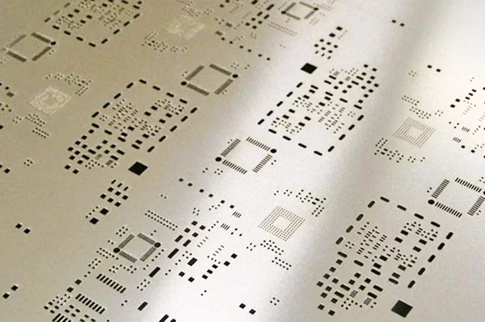
What are stencils? In PCB design and production, stencils are tools used to accurately apply solder paste (or other adhesives) to specific locations on a circuit board. Stencils are typically made from metal (such as stainless steel) or polymer and feature many precisely cut holes or openings. These holes' shapes and locations match the pads and conductive paths required on the circuit board. Through stencils, solder paste can be evenly and accurately applied to the circuit board, ensuring the proper installation and soldering of components.
What are stencils? Stencils play a crucial role in surface mount technology (SMT). SMT is a method of electronic circuit manufacturing where components are directly mounted onto the surface of printed circuit boards (PCBs). Stencils are used to accurately apply solder paste to the pads on the PCB, after which components are placed on the solder paste and permanently fixed to the board through a reflow soldering process. Any inaccuracy in this process can lead to component misalignment or soldering defects, making high-quality stencils essential.The production process of stencils involves using laser cutting or chemical etching techniques to ensure the precision and consistency of the holes. Laser cutting technology uses laser beams to cut stencils, capable of producing very fine and precise holes, while chemical etching forms holes by gradually dissolving unwanted material with a chemical solution. Each of these techniques has its advantages and disadvantages, and the choice of method usually depends on specific application requirements and budget.

What are stencils
An important aspect of using stencils is their maintenance and cleaning. Due to the sticky nature of solder paste, holes can easily become clogged if not cleaned regularly, affecting the precise application of solder paste. Therefore, stencils need to be thoroughly cleaned after each use to ensure they remain effective over time. Additionally, regular inspection and maintenance of stencils are necessary to prevent production issues caused by wear or damage.
What are stencils? In PCB design, the selection and design of stencils are also critical steps. Designers need to determine the size and location of the stencil holes based on the PCB layout and component placement. This often requires using specialized design software to create the stencil template, ensuring it perfectly matches the PCB. Moreover, different types of solder paste and application requirements can also affect the stencil design. For example, high-viscosity solder paste may require larger holes, while low-viscosity solder paste may require smaller holes.Despite the important role stencils play in PCB production, alternative methods are being developed and used. For instance, Direct Printing Technology (DPS) is an emerging technique that uses nozzles to directly spray solder paste onto the PCB pads without needing stencils. This method offers higher flexibility and efficiency in some applications, especially for small-batch or highly variable production needs.
What are stencils? The integration of stencils with automated manufacturing systems is another area of significant development. Automated stencil printers are now equipped with advanced features such as real-time monitoring, automatic alignment correction, and intelligent feedback systems. These advancements help ensure that the solder paste is applied with utmost precision and consistency, reducing the risk of defects and improving overall production efficiency.Environmental and sustainability considerations are also influencing the design and use of stencils. The manufacturing processes for stencils are being optimized to reduce waste and energy consumption. Additionally, the materials used for making stencils are being evaluated for their environmental impact, with a shift towards more sustainable and recyclable options.
In the context of repair and rework, stencils are invaluable tools. When a PCB requires rework, such as replacing a defective component, custom stencils can be created to apply solder paste precisely to the areas needing attention. This ensures that the rework process is as efficient and reliable as the initial manufacturing, maintaining the integrity and performance of the PCB.The future of stencils in PCB production is likely to see further integration with advanced manufacturing techniques such as additive manufacturing and 3D printing. These technologies can produce complex stencil designs that were previously impossible with traditional methods, opening up new possibilities for PCB and electronic device design and production.
what are stencils? Stencils are indispensable tools in PCB design and production, ensuring reliable installation and connection of electronic components through their precise solder paste application capability. As technology advances, the production and use of stencils continue to improve, providing more efficient and reliable solutions for PCB production.