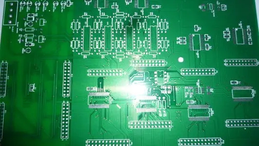
When I saw the PCB of a computer motherboard, I wondered what a great thing to be able to draw by myself. Later, when I came into contact with protel99se, I stepped into the team of the drawing board, and then altium, cadence and so on. With the accumulation of drawing board experience, I found that more and more things need to be paid attention to. A good PCB board is not just to connect the wires. Let me tell the story slowly.

First, most PCB designers are proficient in the working principles of electronic components, know their mutual influence, and understand the various data transmission standards that constitute the input and output of the circuit board. An excellent electronic product requires not only excellent schematics, but also PCB layout and wiring personnel, and the latter plays a vital role in the success or failure of the final PCB board. However, the more a schematic designer knows about excellent layout techniques, the more opportunities there are to avoid major problems.
Second, the layout problem. We all know that the most critical connection design in PCB design is the shortest and most direct path, so that the simplest method can be used to obtain the best results.
Third, the processing of clock signals. It is believed that all those who do PCB design are suffering or preparing to suffer from the problem of clock signal interference. Because the clock line is too long or too long or passes through the signal line, etc., it will amplify the jitter and offset for the downstream, especially when the clock speed increases. First of all, PCB design should avoid using multiple layers to transmit the clock, and do not have vias on the clock line, because vias will increase the impedance change of the trace and the reflection of the signal. Secondly, if the inner layer must be used to lay out the clock, the upper and lower layers should use the ground plane to reduce the delay. Thirdly, if the introduction of clock noise on the power plane will increase the PLL jitter, a "power island" can be created when modifying the PCB design. This technique can use thicker etching in the metal plane to achieve the PLL analog power supply and digital power supply. isolation.
Fourth, the handling of noise issues. With the improvement of PCB design speed, concurrent switching noise, concurrent switching output, ringing, crosstalk ground bounce, power supply noise, etc. also appear. To solve these problems, we must prescribe the right medicine:
A. Ringing and crosstalk. For key signal lines, we must pay attention to crosstalk issues. The commonly used method is to use differential signals and traces with differential pairs. This can fundamentally eliminate the inductive effect and help reduce the "bounce" caused by the induced current in the return path. noise.
B. Use of decoupling and bypass capacitors. In general, decoupling capacitors help reduce the inductance between the PCB's power supply and the ground plane, and control the impedance of signals and ICs everywhere on the PCB. The bypass capacitor provides a clean power supply (provides a charge bank). Usually, we should arrange decoupling capacitors anywhere convenient for PCB wiring. For the use of capacitors, it should be noted that the wiring of decoupling capacitors should be as short as possible.
C. Pay attention to impedance matching. I have done antenna matching circuits, and impedance matching plays a vital role. Now 100Ω characteristic impedance has become the industry standard value for differential connection lines. The 100Ω differential line can be made with two 50Ω single-ended lines of equal length. Since the two traces are close to each other, the field coupling between the wires will reduce the differential mode impedance of the wires. In order to maintain an impedance of 100Ω, the width of the trace must be reduced a bit. As a result, the common mode impedance of each line in a 100Ω differential pair will be slightly higher than 50 ohms. If you really don't want to be so frustrated, when making the PCB, negotiate with the manufacturer what impedance is required for what trace.
Fifth, reference design plan. Now any MCU will give its corresponding reference design. Although these circuit boards are usually designed for multiple purposes, they may not exactly match the design requirements you made. However, they can still be used as a starting point for creating solutions. From this, we can see the routing and positioning of the key parts, which is also a great improvement in the success rate of the design.
The above is a summary of some of my experiences and lessons in PCB design, I hope it will be helpful to everyone. I also hope that everyone can leave me a message and discuss various techniques of PCB design together.