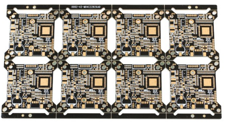
The benefits that the alternative PCBA MCM technology can provide are cost reduction, size reduction, weight reduction, strong environmental adaptability, and fewer interfaces that must be added to improve performance. The advantages of different PCBA MCMs can be applied to different markets. In most situations where PCBA MCM technology is costly, COB provides the cheapest solution. Therefore, COB technology is a better choice in situations where price is prioritized. For example, for consumer electronic products, most handheld calculators use COB technology. However, in many occasions, although the cost of applying PCBA MCM is high, due to the reduction of PCB size and PCB assembly cost, the system cost of using PCBA MCM is reduced.
In aerospace and military applications, the reduction in size and weight that PCBA MCM can achieve is very important, so PCBA MCM is commonly used in spacecraft. Now, notebook computer manufacturers have begun to use PCBA MCM-L technology.
Ceramic hybrid circuit packaging technology is widely used in harsh environments, such as automotive electronics. Ceramic packages are used in occasions that need to be isolated from the external environment.

In addition to notebook computers, some high-performance telecommunications, data processing, network equipment and other devices that require high speed and multiple interfaces are also using PCBA MCM technology. High-end computers have been using PCBA MCM-C for years to increase their operating speed.
Because of the continuous improvement in performance of some low-end systems, especially the increase in multi-processor applications, PCBA MCM will compete for a considerable share of the electronic packaging market. From the perspective of the development trend of PCBA MCM, the most commercial applications in the short term are still portable electronic products. On the other hand, some high-performance single-chip packages may also be changed to PCBA MCM due to the limitation of the number of lead-out pins. In such a system, the reliability is improved due to the reduction of interconnection during the second-level package.
Although it is costly and difficult to solve the KGD problem, PCBA MCM still has a great market driving force. The driving force of low-end products is to reduce size and cost, and the driving force of high-end products is to reduce size and improve performance.
It is estimated that in 2002 the European PCBA MCM market has achieved a large growth, the market is about 4 billion US dollars, during this period the growth momentum is mainly to reduce the size of electronic products. By 2007, the European PCBA MCM market is expected to expand to 10 billion US dollars, and the growth driver is mainly to reduce costs.
5 Low cost PCBA MCM
Driven by the market, with the advancement of design, packaging technology, materials and processes, the cost reduction of PCBA MCM has begun to be realized. In the international market, PCBA MCMs using various standard package outline packages, such as PDIP, QFP, BGA, and so on, have appeared. Different types of PCBA MCM have also adopted various single chip packaging process technologies, such as gold wire bonding, chip bumping and FC technology. Due to the widespread adoption of standard packaging outlines and standard production processes, the packaging cost of PCBA MCM has been greatly reduced.
The thickness of the sputtered multilayer aluminum interconnection layer is usually between 1 to 3 microns. Because the power and ground are connected to the substrate, there are requirements for impedance and reduced coupling. The dielectric (insulating layer) layer consists of 3 to 7 microns thick BCB polymer.
BCB with low dielectric constant can be used stably at THz. In addition to gallium arsenide chips and silicon application specific integrated circuits, the largest application of BCB is wafer-level chip size packaging (WLCSP-Wafer Level Chip Size Package). In addition to the substrate. The substrate and the two chips are from different chip manufacturers.
Including the gold bumps, the internal wiring reaches more than 350 lines. Due to the selection of world-class chips, the PCBA MCM packaged by some PCB factories has first-class quality. It can pass the reliability assessment including 1000 temperature cycles from -40 to 125°C. The pass rate of packaging and testing is up to 99% at 122°C. The package shape is mainly standard PDIP, so the package cost is close to ordinary single-chip IC. Both equipment investment and production capacity can refer to single-chip ICs.
In order to ensure the packaging quality of PCBA MCM, many manufacturers have adopted a variety of new packaging processes in PCBA MCM, such as designing a lead frame with a special structure to solve the thermal endurance of large chips and large packages. There are many issues to consider for PCBA MCM packaging. Choosing such a packaging material can make the BGAPCBA MCM-L withstand the level of thermal shock equivalent to that of a single-chip PQFP.
In order to reduce the packaging cost of PCBA MCM, it is important to select an appropriate packaging method. PCBA MCM packaging methods and characteristics commonly used in mass production are as follows:
Assembly after plastic packaging, low cost and easy assembly
The overall plastic package is suitable for mass production
COB package bare chip and surface mount component package
Metal package, resistant to harsh environments, high package cost
Ceramic package High performance package
The overall plastic packaging method adopted by PCBA MCM is suitable for mass production manufacturers.