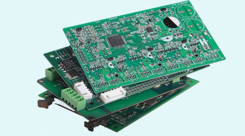
What is etching?
A lead-tin corrosion-resistant layer is pre-plated on the copper foil retained on the outer layer of the circuit board, and then the unprotected non-conductor part of the copper is etched into a circuit by a chemical method.
According to different process methods, etching is divided into inner layer etching and outer layer etching. Acid etching uses wet film or dry film as corrosion resistance, and outer layer etching uses alkali etching. Use tin lead as a corrosion inhibitor.
The basic principle of etching reaction.
1. Acidic copper chloride is corroded.
Development: By using the weak alkalinity of sodium carbonate to preserve the part of the dry film that has not been irradiated with ultraviolet rays.
Etching: According to a certain proportion of the solution, use an acidic copper chloride etching solution to dissolve the dry film or the wet film.
Stripping: Dissolve the protective film on the wire at a certain temperature and speed according to a certain proportion of the medicine.
Acidic copper chloride etching has the characteristics of high etching rate, high etching efficiency, and easy recycling.
2. Alkaline etching.
Film fading: Use the fading Filin solution to remove the film on the circuit board from the unprocessed copper surface.
Etching: Use etching liquid to etch the required bottom copper, leaving thicker lines.. Additives will be used in it. The accelerator is designed to promote the oxidation reaction and prevent the precipitation of copper complex ions; the coastal agent is used to reduce the side corrosion; the inhibitor is used to inhibit the precipitation of ammonia-dispersed copper and accelerate the oxidation reaction of the corroded copper.
New lotion: Use hydrated ammonia without copper ions to remove the remaining liquid on the surface of the board.
Entire hole: This process is only applicable to the golden process of sinking. Mainly remove the excess binding ions in the non-coating pores to prevent sinking in the sinking gold ions.
Tin fade: Use nitrate to remove the tin-lead layer.
Four effects of etching.

Pond effect.
During the PCB etching process, due to gravity, a water film is formed on the board to prevent the new liquid from contacting the copper.
Groove effect.
The adhesion of the liquid makes the gap between the liquid and the circuit cause the difference between the dense area and the open area.
Perforation effect.
The flow of liquid through the holes causes an increase in the rate of liquid renewal around the plate holes.
The swing effect of the nozzle.
The line parallel to the swing direction of the nozzle is easily washed away by the new liquid due to the liquid between the lines, and the liquid is renewed and has a high degree of etching.
The swing direction of the vertical line and the nozzle is because the liquid between the lines is not easily washed away by the new liquid.
Common problems and improvement methods in the etching process.
1. Removal of film.
Due to the low concentration of the medicine, the speed is too fast, the nozzle clogging and other problems will cause film fading. Therefore, it is necessary to check the concentration of the potion and readjust the concentration of the potion to the correct range; adjust the speed parameter in time; and clear the nozzle.
2. PCB surface oxidation.
Because high temperature will cause oxidation of the board surface, it is necessary to adjust the concentration and temperature of the potion in time.
3. The corrosion of copper is not completed.
Because the etching speed is too fast, the composition of the potion is deviated; the copper surface is contaminated; the nozzle is blocked; low temperature will cause copper corrosion. Therefore, it is necessary to adjust the etching transport speed, recheck the chemical composition, pay attention to copper pollution, clean the nozzle, prevent clogging, adjust the temperature and so on.
4. Copper that erodes too high.
Because the machine runs too slowly and the temperature is too high, it will cause excessive copper corrosion, so it is necessary to adjust the speed of the machine to adjust the temperature.
After years of development, ceramic PCB has never stopped exploring in the PCB industry. For example, the thickness of the cover copper can be customized between 1μm and 1mm. The wire diameter can reach 20.m, the hole diameter of laser drilling technology can reach 0.06mm, and the product combination strength can reach 45MPA. It is the only choice for smart power equipment, automotive electronics high-power semiconductor modules, solar panel components, lighting industry, power industry, aerospace and communications industries.
Sliton ceramic circuit board process introduction-perforation.