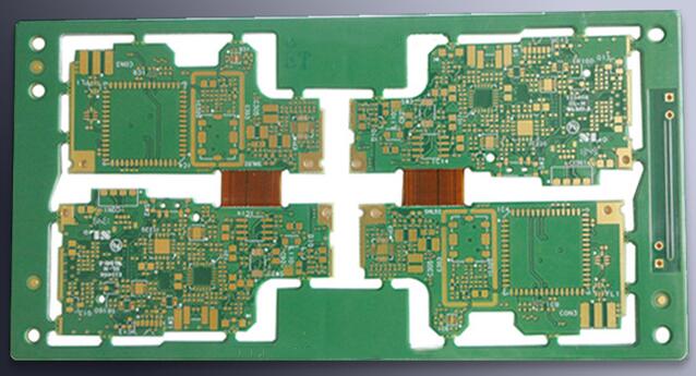
So far, almost all FPC manufacturing processes are performed by subtraction (etching method). According to Cabor technology, copper foil is usually the starting material for forming a corrosion-resistant layer by photolithography, and the surface of the copper foil is removed from the copper surface to form a circuit conductor. Due to problems such as side corrosion during the corrosion process, the etching method has limitations in microcircuit processing.

Then use the splash method to form a crystal planting layer on the polyimide substrate, and then form an anti-corrosion layer pattern of the circuit reverse pattern on the crystal planting layer by photolithography, which is called coating. The conductor circuit is formed by plating on the blank portion. Then remove the corrosion-resistant layer and unnecessary crystal planting layer to form a D-layer circuit. The photosensitive polyimide resin is coated on the D layer circuit, lithography forms holes to form the protective layer or insulating layer used in the second circuit layer, and then sputters on it to form a crystal planting layer as the second layer circuit The conductive layer of the substrate. By repeating the above process, a multilayer circuit board can be formed.
