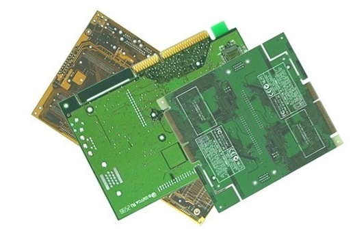
The copper surface area on the circuit board is uneven, which will worsen the bending and warping of the board.
1. Generally, a large area of copper foil is designed on the circuit board for grounding purposes. Sometimes there is also a large area of copper foil designed on the Vcc layer. When these large area copper foils cannot be evenly distributed on the same sheet When the circuit board is used, it will cause the problem of uneven heat absorption and heat dissipation. Of course, the circuit board will also expand and contract. If the expansion and contraction cannot be performed at the same time, it will cause different stress and deformation. When the upper limit of the Tg value is reached, the board will begin to soften, causing permanent deformation.
2, the connection points (vias, vias) of each layer on the circuit board will limit the expansion and contraction of the board.
Today's circuit boards are mostly multi-layer boards, and there will be rivet-like connection points (vias) between the layers. The connection points are divided into through holes, blind holes and buried holes. Where there are connection points, the board will be restricted. The effect of expansion and contraction will also indirectly cause plate bending and plate warping.

PCB circuit board impedance refers to the parameters of resistance and reactance, which hinder the alternating current.
In the production of PCB circuit boards, impedance processing is essential. The reasons are as follows:
1. The PCB circuit (bottom of the board) should consider plugging and installing electronic components. After plugging, the conductivity and signal transmission performance should be considered. Therefore, the lower the impedance, the better, and the resistivity should be less than 1 per square centimeter. -6 or less.
2. In the production process of PCB circuit boards, they have to undergo PCB process manufacturing links such as copper sinking, electrolytic tin plating (or chemical plating, or thermal spray tin), connector soldering, and the materials used in these links must ensure that the resistivity is low. Ensure that the overall impedance of the circuit board is low to meet the product quality requirements and can operate normally.
3. The tin plating of PCB circuit boards is the most prone to problems in the production of the entire circuit board, and it is a key link that affects impedance. The biggest defect of the electroless tin coating is easy discoloration (easy to be oxidized or deliquescent) and poor solderability, which will lead to difficult soldering of the circuit board, high impedance, poor electrical conductivity, or instability of the overall board performance.
4. There are various signal transmissions in the conductors in the PCB circuit board. When it is necessary to increase its frequency in order to increase its transmission rate, if the circuit itself is different due to factors such as etching, stack thickness, wire width, etc., the impedance value will change., So that its signal is distorted and the performance of the circuit board is degraded, so it is necessary to control the impedance value within a certain range.