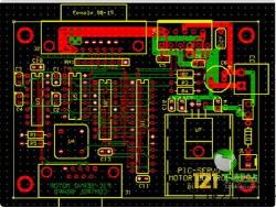
Dry film photoresist is a pre-prepared liquid photoresist (Photoresist) uniformly coated on the carrier polyester film (PET film) on a precision coating machine and under high cleanliness conditions, after drying and cooling Then, it is covered with a polyethylene film (PE film) and wound into a roll-shaped film-type photoresist. It is a special chemical for PCB photoresist for PCB factory.
The dry film photoresist is pressed on the copper clad board, and the circuit pattern on the negative film (mask or negative plate) is copied to the dry film photoresist through exposure and development, and then the dry film photoresist is used for anti-etching Performance, the copper clad laminate is etched to form the fine copper circuit of the printed circuit board. The performance of dry film photoresist is mainly determined by the chemical composition of the photoresist layer.

The dry film photoresist layer is composed of three main chemicals: resin, photoinitiator, and monomer. The resin is used as a film-forming agent to bond the components of the photoresist into a film. The resin is required to have good mutual solubility with each component and good adhesion to the processed metal surface. It should be easy to use alkali from the metal surface. Removal from solution has good corrosion resistance, electroplating resistance, cold flow resistance, heat resistance and other properties.
The photoinitiator absorbs ultraviolet light of a specific wavelength (usually 320-400nm) and then cleaves by itself to generate free radicals. The free radicals further initiate the crosslinking of the photopolymerizable monomer. The photoinitiator has a decisive influence on the photosensitive speed, exposure time latitude and deep curability of the dry film photoresist. With the continuous progress and changes of light source technology, customers' requirements for the photosensitive performance of dry film photoresists continue to increase, and the requirements for the type, chemical structure, performance and quality of photoinitiators are also constantly changing.
The function of the photo-imaging solder resist ink is to prevent short circuits caused by solder laps, form a permanent protective layer for the circuit, and ensure the safety and electrical performance of the printed circuit board in the production, transportation, storage, and use. Photographic solder resist ink is one of the most critical materials for PCB manufacturing. The advent of the first generation of solder resist-two-component thermosetting solder resist in the 1960s accelerated the development of the PCB industry. Subsequently, in order to adapt to the changes in market demand, after continuous improvement and update, the second generation of solder resists, namely light-curable (UV light-cured) solder resists, appeared, and was widely used. In recent years, in order to meet the needs of manufacturing high-density PCBs, the third-generation solder resist, that is, liquid photoimageable solder resist ink, has been developed. Its main components are epoxy resin, monomers, prepolymers, photoinitiators (including light Sensitizer), colorant, etc., due to the structure of the prepolymer, there are groups that can be photopolymerized and there are groups that can be thermally crosslinked. Through exposure and development, high registration accuracy can be obtained After heating and cross-linking, the solder mask is denser and smoother, and its heat resistance, insulation and other physical and electrical properties are better. It is currently the mainstream application product. Among them, the photoinitiator plays an important role in imaging performance.