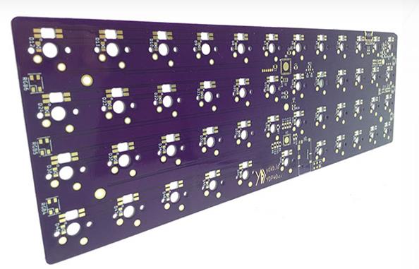
PCB land (land), the basic unit of surface mount assembly, is used to form the land pattern of the circuit board, that is, a variety of land combinations designed for special PCB component types. There is nothing more frustrating than a poorly designed pad structure. When a pad structure is not designed correctly, it is difficult, sometimes even impossible, to reach the expected solder joint. There are two words in English for pad: Land and Pad, which can often be used interchangeably; however, in terms of function, Land is a two-dimensional surface feature used for surface mountable components, while Pad is a three-dimensional feature used for The components of the plug-in. As a general rule, Land does not include plated through-holes (PTH, plated through-hole). Bypass holes (via) are plated through holes (PTH) that connect different circuit layers. Blind vias connect the outermost layer with one or more inner layers, while the buried vias only connect the inner layer.
As noted earlier, PCB land land usually does not include plated through holes (PTH). The PTH in a land land will take away a considerable amount of solder during the soldering process, resulting in insufficient solder joints in many cases. However, in some cases, PCB design component wiring density forces to change to this rule, most notably for chip scale package (CSP, chip scale package). Below 1.0mm (0.0394") pitch, it is difficult to route a wire through the "labyrinth" of the pad. Blind bypass holes and microvias (microvia) are created in the pad, allowing direct wiring to another layer .Because these by-pass holes are small and blind, they will not suck too much solder away, resulting in little or no effect on the amount of tin in the solder joints.

There are many industry documents from IPC (Association Connecting Electronics Industries), EIA (Electronic Industry Alliance) and JEDEC (Solid State Technology Association), which should be used when designing the pad structure. The main document is IPC-SM-782 "Surface Mount Design and Land Structure Standard", which provides information about land structures for surface mount components. When J-STD-001 "Requirements for Soldering Electrical and Electronic Assembly" and IPC-A-610 "Acceptability of Electronic Assembly" are used as solder joint process standards, the pad structure should meet the intent of IPC-SM-782. If the pad deviates greatly from IPC-SM-782, it will be difficult to achieve a solder joint that meets J-STD-001 and IPC-A-610.
"Component knowledge (ie, component structure and mechanical size) is a basic requirement for the design of the pad structure. IPC-SM-782 widely uses two component documents: EIA-PDP-100 "Registration and Standard Mechanical Shape of Electronic Parts" and JEDEC 95 publication "Registration and Standard Shape of Solid and Related Products". Indisputably, the most important of these files is the JEDEC 95 publication, because it handles the most complex components. It provides mechanical drawings of all registrations and standard appearances of solid components.
defines component abbreviations based on package characteristics, materials, terminal location, package type, pin form, and number of terminals. Characteristic, material, location, form and quantity identifiers are optional.
Package feature: A single or multiple letter prefix that identifies features such as pitch and outline.
Packaging material: A one-letter prefix to identify the main packaging material.
Terminal location: A single letter prefix that confirms the terminal location relative to the package outline.
Package type: A two-letter mark that indicates the package shape type.
New pin style: a single letter suffix to confirm the pin style.
Number of terminals: a one-, two-, or three-digit number suffix to indicate the number of terminals.
A simple list of surface mount package feature identifiers includes:
E Expand the spacing (>1.27 mm).
F Close pitch (<0.5 mm); limited to QFP components.
S Shrink spacing (<0.65 mm); all components except QFP.
T thin type (1.0 mm body thickness).
A simple list of surface mount terminal location identifiers includes:
Dual pins are on opposite sides of a square or rectangular package.
The Quad pins are on the four sides of a square or rectangular package.
A simple list of package type identifiers for surface mount includes:
CC chip carrier (chip carrier) package structure.
FP flat pack package structure.
GA grid array packaging structure.
SO small outline package structure.
A simple list of pin format identifiers for surface mount includes:
B A straight shank or spherical pin structure; this is a non-compliant pin form
F A straight pin structure; this is a non-compliant pin form
G A wing-shaped pin structure; this is a compliant pin form
J A "J"-shaped bent lead structure; this is a compliant lead form
N A pinless structure; this is a non-compliant pin form
S An "S"-shaped pin structure; this is a compliant pin form
"For example, the abbreviation F-PQFP-G208 describes a 0.5 mm (F) plastic (P) square (Q) flat package (FP), fin-shaped pin (G), and the number of terminals 208.
Detailed tolerance analysis of PCB components and board surface features (ie pad structure, reference points, etc.) is necessary. PCB manufacturing IPC-SM-782 explains how to perform this analysis. Many components (especially fine-pitch components) are designed in strict metric units. Do not design imperial pad structures for metric components. Accumulated structural errors produce mismatches and cannot be used for close-pitch components at all. Remember, 0.65mm is equal to 0.0256" and 0.5mm is equal to 0.0197".