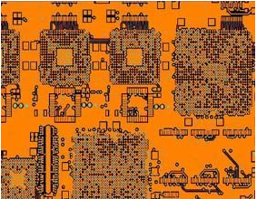
PCB design is not an arbitrary thing, there are many specifications that need to be followed by designers.
Basic principles of layout
1. Communicate with relevant personnel to meet special requirements in terms of structure, SI, DFM, DFT, and EMC.
2. According to the structural element diagram, place the components that need to be positioned such as connectors, mounting holes, indicator lights, and give these components non-movable attributes, and carry out dimensions.
3. According to the structural element diagrams and the special requirements of certain devices, set up no-wiring area and no-layout area.
4. Comprehensive consideration of PCB performance and processing efficiency to select the process flow (preferably single-sided SMT; single-sided SMT + plug-in; double-sided SMT; double-sided SMT + plug-in), and layout according to the characteristics of different processing technology.
5. Refer to the results of the pre-layout when layout, according to the layout principle of "big first, then small, first difficult then easy".
6. The PCB layout should meet the following requirements as far as possible: the total wiring is as short as possible, and the key signal line is the shortest; high voltage, large current signals and low voltage, low current signals are completely separated from weak signals; analog signals and digital signals are separated; high Separate high-frequency signals from low-frequency signals; the spacing of high-frequency components should be sufficient. Under the premise of meeting the requirements of simulation and timing analysis, local adjustments are made.
7. As far as possible, the same circuit part adopts a symmetrical modular layout.
8. The recommended grid for layout setting is 50mil, and for IC device layout, the recommended grid is 25 25 25 25 mil. When the layout density is high, the grid setting of small surface mount devices is recommended to be no less than 5mil.
9. When layout, consider the position of fanout and test points, move with reference to the center point of the device, and consider running two traces between the two vias.
1. The number of printed conductor wiring layers is determined according to needs. The wiring occupied channel ratio should generally be more than 50%;
2. According to the process conditions and wiring density, select the wire width and wire spacing reasonably, and strive for uniform wiring within the layer, and the wiring density of each layer is similar. If necessary, auxiliary non-functional connection pads or printed wires should be added to the lack of wiring areas;
3. Two adjacent layers of wires should be laid out perpendicular to each other and diagonally or bent to reduce parasitic capacitance;

4. The wiring of printed wires should be as short as possible, especially high-frequency signals and highly sensitive signal lines; for important signal lines such as clocks, delay wiring should be considered when necessary;
5. When multiple power sources (layers) or ground (layers) are arranged on the same layer, the separation distance should not be less than 1mm;
6. For large area conductive patterns larger than 5*5mm2, windows should be partially opened;
7. Thermal isolation design should be carried out between the large-area graphics of the power supply layer and the ground layer and their connection pads, as shown in Figure 10, so as not to affect the welding quality.
Line width/line spacing of trace
1. The recommended line width/spacing is ≥5mil/5mil, and the minimum usable line width/spacing is 4mil/4mil.
2. The distance between the trace and the pad: The distance between the outer trace and the pad is consistent with the distance between the inner trace and the ring.
3. The distance between the outer trace and the pad must meet the requirement that the distance between the trace and the solder mask opening edge of the pad is ≥2mil.
Safety distance for routing
1. The distance between the trace and the edge of the board>20mil. The distance between the inner power/ground and the edge of the board>20mil.
2. The distance between the grounding bus line and the grounding copper foil must be more than 20 mils from the edge of the board.
3. No wiring is allowed in areas where metal shells (such as radiators, power modules, metal handles, horizontal voltage regulators, crystal oscillators, ferrite inductors, etc.) directly contact the PCB. The contact area between the metal shell of the device and the PCB extends 1.5mm to the outside for the surface wiring forbidden area.
The shortest distance between the trace and the non-metallized hole
The general principle of multi-layer PCB layer layout
1. The bottom of the device surface (the second layer) is the ground plane, which provides a device shielding layer and a reference plane for wiring on the device surface;
2. All signal layers are as close as possible to the ground plane;
3. Try to avoid two signal layers directly adjacent to each other;
4. The main power supply is as close as possible to it correspondingly;
5. In principle, a symmetrical structure design should be adopted. The meaning of symmetry includes: the thickness and type of the dielectric layer, the thickness of the copper foil, and the pattern
Symmetry of distribution type (large copper foil layer, circuit layer).
General requirements for silk screen design
1. In order to ensure that all letters, numbers and symbols are easy to identify on the PCB, the line width of the silk screen must be greater than 5 mils, and the height of the silk screen should be at least 50 mils.
2. The silk screen is not allowed to overlap with the pad and the reference point.
3. White is the default silk screen ink color. If there are special requirements, it needs to be explained in the PCB drilling drawing file.
4. In high-density PCB design, the content of silk screen printing can be selected according to needs.
5. The arrangement direction of silk-screened strings is from left to right and from bottom to top.