In PCB design, Design Rule is the key to the success or failure of a PCB design. The intent of all PCB designers and the functional manifestation of PCB design are driven and realized by the soul of PCB design rules. Exquisite and meticulous rule definitions can help designers in the work of PCB layout and routing, save engineers a lot of energy and time, help PCB designers achieve excellent PCB design, and greatly facilitate PCB design work.
The entire PCB design needs to comply with the rule definition. Including the most basic electrical rules (spacing, short circuit and open circuit), PCB wiring rules (line width, wiring style, via style, fan-out, etc.), plane rules (power ground plane layer connection method, copper connection method); and Other commonly used auxiliary rules such as layout rules, manufacturing rules, high-speed PCB board design rules, signal integrity rules and so on. After the PCB design is completed, the Design Rule Check can also be performed to re-examine the PCB design to see if there is any violation of the rules and to improve and perfect it.

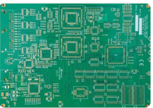
PCB
Rules and skills on PCB copper design. Introduce how to change the connection method of copper and vias and shrink the board edge when designing copper in Altium Designer.
How to connect the via hole after copper is not crisscross like the thermal pad
If you want to make the through-hole connections in the copper-paved PCB board not cross-shaped, but directly connected, you can set it in the Plane-Polygon connect style item in the Design Rule. The default setting above is Relief connection, which is a cross pattern connection like a thermal pad. A rule is added, and the object is set to all vias IsVia in the Query statement. The rule is set to direct connection. After re-plating the copper. The cross-shaped pattern connection is cancelled.
Set different spacing for copper paving (board edge shrinkage)
In the PCB design and manufacturing industry, under normal circumstances, due to the mechanical considerations of the finished circuit board, or to avoid the curling or electrical short circuit that may be caused by the exposed copper skin on the edge of the board, engineers often place large areas of copper relative to Shrink the edge of the board by 20 mils instead of spreading the copper to the edge of the board. There are many ways to deal with this kind of copper shrinkage. For example, draw a keepout layer on the edge of the board, and then set the distance between the copper paving and the keepout. A simple method is introduced here, that is, to set different safety distances for copper paving objects. For example, the safety distance of the entire board is set to 10 mils, and the copper paving is set to 20 mils. It can achieve the effect of 20mil shrinkage of the edge of the board. At the same time, dead copper that may appear in the device is removed. Do multiple things in one fell swoop.
There are many ways to deal with the indentation of the edge of the PCB board design. It is more clear and convenient to use the Query statement to accurately set the copper paving object.