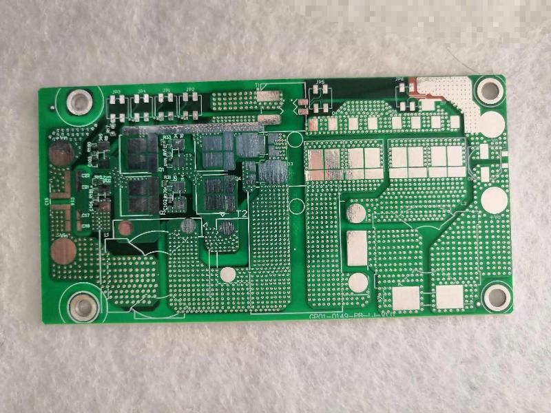
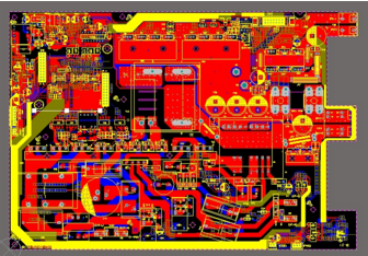
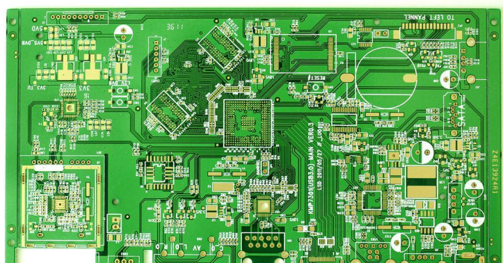
What is high speed PCB design?High speed PCB design refers to the circuit board design that can support high-speed signal transmission, these signals usually refer to high-speed digital signals, high-speed analogue signals and so on. High-speed PCB design in the choice of materials, layout design, wiring design and other aspects of special requirements to ensure that the integrity and stability of the signal in the transmission process, the signal in the transmission process is not distorted, does not attenuate, and to meet the performance requirements of the system.
What is a high-speed signal?
In response to this question, Cadence, a world-renowned EDA software company, defines it:
Any signal greater than 50MHz is a high-speed signal;
When the transmission path length of the region where the signal is located is greater than 1/6λ, it will be identified as a high-speed signal;
Whether the signal is high-speed or not is independent of the frequency, and the general default: a signal is considered high-speed when its rising/falling edge is less than 50ps;
When the signal is transmitted along the transmission path, it can be considered as a high-speed signal if serious skin effect and power loss occur.

What is high speed circuit
It is generally considered that if the digital logic circuit frequency reaches or exceeds 45MHZ~50MHZ, and the circuit operating above this frequency has accounted for a certain amount of the entire electronic system (say, 1/3), it is called high-speed circuit.
In fact, the harmonic frequency of the edge of the signal is higher than that of the signal itself. It is the rising edge and falling edge (or jump of the signal) that causes the unexpected result of signal transmission. Therefore, it is generally agreed that if the line propagation delay is greater than the rise time of the driving end of 1/2 digital signal, such signal is considered to be high-speed signal and produce transmission line effect.
Signal transmission occurs at the moment when the state of the signal changes, such as the time of rise or fall. The signal passes through a fixed period of time from the driver to the receiver. If the transmission time is less than 1/2 of the rise or fall time, the reflected signal from the receiver will reach the driver before the signal changes state. Conversely, the reflected signal will arrive at the driver after the signal changes state. If the reflected signal is strong, the superimposed waveform may change the logical state.
Determination of high-speed signals
Above we have defined the preconditions for the occurrence of transmission line effect, but how to know whether the line delay is greater than 1/2 of the signal rise time of the driver? In general, the typical value of the signal rise time can be given in the device manual, and the signal travel time in PCB design is determined by the actual wiring length. The figure below shows the correspondence between signal rise time and allowable wiring length (delay).
The delay per unit inch on the PCB is 0.167ns. However, if there are many holes, pins, and constraints on the network cable, the delay will increase. Typically, the signal rise time for high-speed logic devices is about 0.2ns. If there is GaAs chip on the board, the large wiring length is 7.62mm.
Set Tr as signal rise time and Tpd as signal line propagation delay. If Tr≥4Tpd, the signal falls in the safe zone. If 2Tpd≥Tr≥4Tpd, the signal falls in the uncertainty region. If Tr≤2Tpd, the signal falls in the problem area. For signals falling in uncertain and problem areas, high-speed wiring methods should be used.
What is transmission line
The wiring on the PCB board can be equivalent to the series and parallel capacitance, resistance and inductance structure shown below. Typical values for series resistances are 0.25-0.55 ohms/foot. Parallel resistances are usually very high because of the insulation layer. After the parasitic resistance, capacitance, and inductance are added to the actual PCB wiring, the final impedance on the wiring is called the characteristic impedance Zo. The wider the wire diameter, the closer it is to the power/ground, or the higher the dielectric constant of the isolation layer, the smaller the characteristic impedance. If the impedance of the transmission line and the receiving end do not match, the output current signal and the final stable state of the signal will be different, which causes the signal to be reflected at the receiving end, which will be sent back to the signal transmitter and reflected back again. As the energy decreases, the amplitude of the reflected signal will decrease until the voltage and current of the signal stabilize. This effect is called oscillations, and oscillations of the signal are often seen at the rising and falling edges of the signal.
Transmission line effect
Based on the transmission line model defined above, it can be concluded that the transmission line will have the following effects on the overall circuit design.
· Reflected signals Reflected signals
· Delay & Timing errors
· Multiple logic level threshold crossing errors False Switching
· Overshoot and Undershoot
· Induced Noise (or crosstalk)
· EMI radiation
Reflected Signal
If a line is not terminated correctly (terminal matching), the signal pulse from the driver is reflected at the receiver, causing an unexpected effect that distorts the signal profile. When the distortion distortion is very significant, it can lead to a variety of errors, resulting in design failure. At the same time, the distortion of the signal to noise sensitivity increased, will also cause design failure. If the above situation is not considered enough, EMI will increase significantly, which will not only affect the design results, but also cause the failure of the whole system.
The main causes of reflected signals are as follows: too long wiring; Unmatched terminated transmission lines, excess capacitance or inductance, and impedance mismatches.
Delay and timing errors
Signal delay and timing errors are: the signal remains unchanged for a period of time when the signal changes between the high and low thresholds of the logic level. Excessive signal delay may lead to timing errors and device dysfunction.
Problems usually occur when there are multiple receivers. The circuit designer must determine the time delay in the bad case to ensure the design is correct. Cause of signal delay: The driver is overloaded and the cable is too long.
Multiple Logic level crossing threshold Errors
The signal may cross the logical level threshold several times during hopping, resulting in this type of error. Multiple crossing the logic level threshold error is a special form of signal oscillation, that is, signal oscillation occurs near the logic level threshold, multiple crossing the logic level threshold will lead to logic dysfunction. Reflected signals are caused by: too long wiring, unterminated transmission lines, excess capacitance or inductance, and impedance mismatches.
Overshoot and downshoot
Overshoot and downshoot come from two reasons: too long line or signal change too fast. Although most element receivers are protected by input protection diodes, sometimes these overshoot levels can exceed the supply voltage range of the element, damaging the element.
Crosstalk
Crosstalk means that when a signal passes through one signal line,relevant signals will be induced on the adjacent signal lines on the PCB board,which is called crosstalk.
The closer the signal cable is to the ground cable, the larger the distance between the lines is, and the smaller the crosstalk signal is generated. Asynchronous signals and clock signals are more prone to crosstalk. Therefore, the method of eliminating crosstalk is to remove the crosstalk signal or shield the seriously disturbed signal.
Electromagnetic Radiation
Electro-Magnetic Interference (EMI),which causes excessive electromagnetic radiation and sensitivity to electromagnetic radiation.EMI indicates that when a digital system is powered on, it radiates electromagnetic waves to the surrounding environment,thus interfering with the normal operation of electronic devices in the surrounding environment.The main reason is that the circuit working frequency is too high and the layout and wiring is unreasonable. At present, there are software tools for EMI simulation,but EMI emulators are very expensive and it is difficult to set simulation parameters and boundary conditions, which will directly affect the accuracy and practicability of simulation results. The common practice is to apply the design rules controlling EMI to each link of the design to realize the rule driving and control in each link of the design.
High speed pcb design essentials: layout and wiring guide
Reasonable specification of the layout and wiring, is to ensure signal integrity, to prevent crosstalk, radiation and impedance discontinuity and other common EMI problems. The following specifications can be greater to avoid a series of problems in high speed PCB design.
1.Ground layer, power layer and stacking layer: Ensure that the PCB stacked under the high-speed transmission line has a uniform ground, and will not go through the ground / power layer gap.
2.Characteristic Impedance: Specific alignment widths should be enforced in the transmission line to ensure that the characteristic impedance and input impedance have specific values on the high-speed interconnect.
3.Transmission line spacing: Maintain adequate spacing between alignments on the PCB to prevent significant crosstalk and to ensure that signals do not exceed the noise tolerance of the receiver.
4.Power Integrity: Place power and ground layers side-by-side, especially the portion of the PDN that powers high-speed components to prevent excessive ringing.
5.Bus and Differential Pair Routing: Enforce timing matches on parallel buses and differential pairs to ensure minimal deviation between critical signals.
6.Component Placement: Ensure that critical high-speed components are placed in the PCB layout so that all critical signals can be routed with minimal layer transitions.