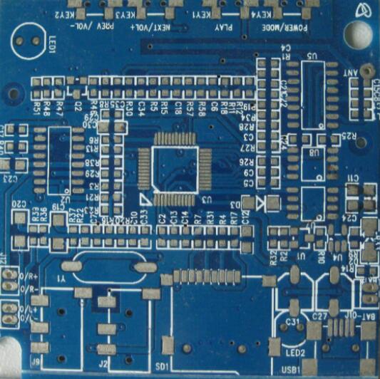
The generation of crosstalk in PCB design and how to avoid it
A changed signal (such as a step signal) propagates along the transmission line from A to B, and a coupled signal will be generated on the transmission line CD. Once the changed signal ends, that is, when the signal returns to a stable DC level, the coupled signal does not exist, so crosstalk It only occurs in the process of signal transitions, and the faster the signal edge changes (conversion rate), the greater the crosstalk generated.
The electromagnetic field coupled in space can be extracted as a collection of countless coupling capacitors and coupling inductances. The crosstalk signal generated by the coupling capacitor can be divided into forward crosstalk and reverse crosstalk Sc on the victim network. These two signals have the same polarity; The crosstalk signal generated by the inductance is also divided into forward crosstalk and reverse crosstalk SL, and these two signals have opposite polarities.
The forward crosstalk and reverse crosstalk produced by the coupling inductance and capacitance exist at the same time, and the magnitudes are almost equal. In this way, the forward crosstalk signals on the victim network cancel each other due to the opposite polarity, and the reverse crosstalk polarity is the same, and the superposition is enhanced. The modes of crosstalk analysis usually include default mode, three-state mode and worst-case mode analysis.

The default mode is similar to the way we actually test the crosstalk, that is, the offending network driver is driven by a flip signal, and the victim network driver maintains the initial state (high level or low level), and then the crosstalk value is calculated. This method is more effective for crosstalk analysis of unidirectional signals. The tri-state mode means that the driver of the offending network is driven by a flip signal, and the tri-state terminal of the victim network is set to a high-impedance state to detect the size of the crosstalk. This method is more effective for two-way or complex topology networks. The worst-case analysis refers to keeping the driver of the victim network in the initial state, and the simulator calculates the sum of the crosstalk of all the default infringement networks to each victim network.
This method generally only analyzes individual critical networks, because there are too many combinations to be calculated and the simulation speed is relatively slow.
Over the years, we are proud to maintain a 99% on-time delivery rate. We work in three shifts to ensure that your PCB can appear on your desk as planned and as early as possible. You can choose DHL and other courier services to balance speed and budget. We only use services from reliable and reputable companies.
24 hours customer service
Whenever you encounter any problems, you can contact the on-site customer service staff to reply to your emails or messages. From the moment you submit the Gerber file to the moment you receive the PCB and assembled PCB, our service staff will follow up your order with satisfaction.
Customer complaints and refunds