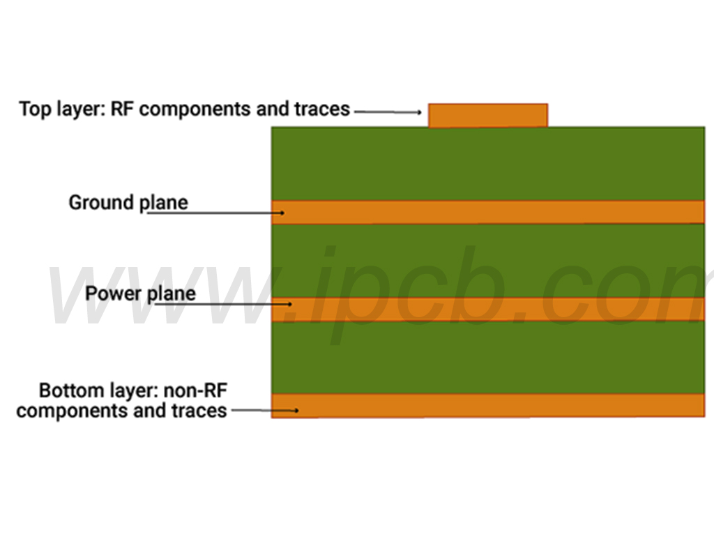
RF PCB stackup is a design method in which multiple printed circuit board (PCB) layers are stacked together in a specific structure to realize the connection and functionality of electronic components. Through stacking, designers are able to increase the density of the board in a limited space while realizing diverse functions, which is especially important in modern electronic devices.
Key components of RF PCB stackup:
Signal Layers:Typically,signal layers are used to carry RF signals,and these layers need to be designed with impedance matching and signal integrity in mind.
Ground Layer:In order to ensure signal stability and reduce EMI (Electro Magnetic Interference), the ground layer layout must be laid out over a large area, including a complete ground plane above and below the signal layer.
Power Layer:The power layer is usually laid out near the signal layer to provide stable power and maintain good power integrity.A good configuration between the ground plane and the power layer also has a significant impact on signal quality.
Insulation Layers:Insulation layers are used to isolate the different signal and power layers to prevent interference.These layers are usually made of dielectric materials and affect the high frequency performance and impedance control of the circuit.
Vias:In the design process,vias are an important part of connecting the various layers.Minimizing the use of vias helps to reduce signal reflection and loss.
Principles to follow in RF PCB stackup design:
Ground management:Usually,the main ground plane is arranged in the second layer of the stack,and the RF signal lines should be arranged in the top layer.This can effectively reduce signal interference and optimize the return path of the signal.
Arrangement of signal and power layers:Reasonable layout of the signal and plane layers helps provide good impedance matching and signal stability, ensuring that reflections and losses are minimized during signal transmission.
Reducing the use of vias:Reducing the size of vias in the RF path reduces signal reflections and losses,which in turn improves overall signal integrity and transmission efficiency.
The characteristics of RF signals require designers to focus on the following points when stacking:
Impedance matching: The width of the signal line and the design of adjacent layers need to meet impedance matching in order to minimize signal reflection and loss.
Thermal performance: high-frequency signals are often accompanied by a large power output, so you need to design a reasonable thermal structure to ensure the stability of the circuit board.
EMI suppression: reasonable layer arrangement and good grounding design can effectively reduce electromagnetic interference and improve the anti-interference ability of the PCB.

Strategies to improve the signal integrity of RF PCB stackup:
1.Optimize the layer stacking configuration
The layer stack configuration of RF PCBs should be reasonably designed to ensure the proper distance between the signal layer and the ground plane. This configuration can provide a good reference plane, reduce signal reflection and interference, and improve signal integrity.
2.Use appropriate materials
When selecting PCB materials, using materials with low dielectric constant and low loss factor can significantly improve the speed and quality of signal propagation. In addition, the materials used in multilayer PCB design should have excellent impedance characteristics to ensure the stability of high-frequency signals.
3. Reduce the length of the alignment
The length of the signal alignment should be shortened as much as possible,which can reduce the signal delay and loss. In PCB design,optimize the alignment path to avoid unnecessary holes and corners to maintain signal integrity.
4.Increase grounding layer
Properly configured grounding layer not only reduces electromagnetic interference (EMI), but also provides a good signal return path and enhances signal stability. The use of multiple grounding layers can improve the power distribution network (PDN), which in turn improves signal integrity.
5.Apply impedance matching technology
The design should ensure that the characteristic impedance of the signal line matches the source and load impedance to minimize signal reflection. When wiring, the required impedance matching can be achieved by adjusting the alignment width and distance between layers.
6.Implement a good wiring strategy
Applying matching impedance termination and proper wiring spacing can effectively reduce radiation and crosstalk. When wiring, you can refer to the principles and methods of existing good design to ensure that the signal can be effectively transmitted in the PCB.
7.Signal integrity analysis
The importance of signal integrity analysis should not be ignored. Through the use of professional analysis tools, designers can simulate and predict the signal integrity performance of the PCB substrate in the operating conditions, and according to the results of the analysis of the necessary adjustments.
RF PCB stackup is a crucial design aspect of modern electronic devices. Proper stacking design not only improves circuit density and functionality, but also effectively addresses challenges such as signal integrity, impedance matching, and electromagnetic interference. By following the principles of ground management, optimizing layer stack configurations, using appropriate materials, and reducing alignment lengths, designers can significantly improve the performance of RF PCBs.