
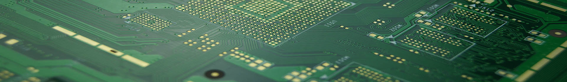

RF PCB routing refers to the process of routing in RF circuit board design, which usually involves the layout and design of high-frequency signal transmission. RF signals are electromagnetic waves in the range of 30MHz to 10GHz and are widely used in wireless communications, radar, RFID and other fields. Due to the characteristics of RF signals, wiring requirements are high to ensure signal integrity and reliability.
Steps of RF PCB routing
1.Function and demand analysis
Before starting the design, the function of the PCB should be analyzed in detail, including the operating frequency band, current and voltage and the main RF device types. In addition, should also consider the board's electromagnetic compatibility (EMC) and related RF indicators, in order to lay the foundation for subsequent design.
2.Material selection and laminated structure
Selection of PCB materials suitable for high-frequency applications, the laminated structure of the board for a reasonable design. The choice of material not only affects the signal loss, but also has an important impact on impedance matching and electromagnetic interference. In addition,the stacking structure should be clearly defined in order to optimize the signal propagation path.
3.Component Layout
In the layout stage, the placement of components should follow certain principles, such as RF signal path components should be as close as possible and neatly arranged to reduce the length of the alignment and avoid cross-interference. High-power circuits and low-power circuits should be separated as much as possible, and sensitive analog signals should be kept away from high-speed digital signals and RF signals to ensure signal stability.
4.Cabling design
In wiring, should ensure that the RF signal alignment as short and straight as possible to reduce the line of mutation, minimize the use of over-hole, as well as to avoid intersecting with other signal lines. RF signal lines should be arranged around the grounding point, improve the grounding effect, in order to reduce noise and interference.
5.Impedance matching
The design should ensure that the impedance of the circuit is matched to minimize signal reflection and loss. Specifically, the width and thickness of the RF alignment should be reasonably designed based on the characteristics of the material to meet specific impedance requirements.
6.Safety check and simulation
After completing the preliminary design, the design should be subject to a number of safety checks and simulations to confirm the signal integrity and circuit reliability. Using professional simulation tools, potential problems can be identified and necessary adjustments and improvements can be made.
7.Final Optimization and Manufacturing
After confirming that the design is correct, final optimization and preparation of relevant documents are carried out, and then the design is submitted to the PCB manufacturer for production. This stage should also consider the feasibility of the manufacturing process to ensure that the design in the actual application of the implementation of the effect.

RF PCB routing key principles
1.Avoid parallel lines
In RF PCB design, parallel wiring is usually not recommended, especially the signal path should be minimized. If you do need parallel wiring, you must add a ground line between the two lines to ensure good grounding, thereby reducing signal interference.
2.Control the length of the wiring
RF signal transmission rate is extremely fast, so the length of the wiring needs to be as short as possible to reduce signal delay and power loss. The design needs to accurately control the width and spacing of the line to achieve impedance matching.
3.Electrical Partitioning
In the layout, the power supply, digital circuits and analog circuits are usually separated to avoid cross-area routing. Digital and analog circuits should be kept at a distance to reduce the signal loop area and improve anti-interference capability.
4.Use large area grounding
As much grounding as possible should be arranged on each layer and connected to the main ground. This enhances signal integrity and reduces electromagnetic interference. Good grounding design is an important factor in ensuring signal quality.
5.Adopt reasonable isolation measures
In the design, key modules such as crystal oscillators, filters and amplifiers should be isolated from low-power modules as much as possible to minimize mutual interference. Reasonable layout and ground plan can improve system performance.
6.Ensure Signal Integrity
RF alignments should not normally be perforated, but if a layer change is required, the aperture size should be minimized to reduce path inductance and signal leakage. At the same time, additional grounding should be arranged around the alignment to reduce coupling between signals.
7.Use of lights
In high-frequency applications, the design should ensure that the line width of 10 mil or more to avoid phase errors, and as far as possible to make the line length and the distance between the lines are equal. This is critical to the stability of the RF signal.
RF PCB routing is a key link in the design of high-frequency circuits, involving multiple steps from functional analysis,material selection to impedance matching and simulation. Reasonable routing not only improves signal integrity and reliability, but also effectively reduces interference and loss.


