

PCB laser etching is increasingly being applied in the design and production of printed circuit boards (PCBs). As electronic products continue to evolve towards miniaturization and higher density, This technology has become an indispensable part of modern electronic manufacturing due to its high precision and efficiency. This article will explore the principles, advantages, and applications of This technology in real-world production.
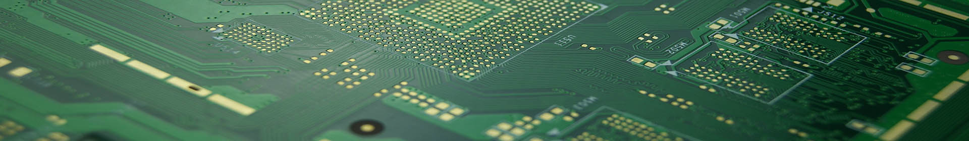
PCB laser etching is a process that uses a laser beam to etch patterns on the surface of a PCB. Unlike traditional chemical etching, laser etching does not require corrosive chemicals but instead uses high-energy laser beams to precisely remove unwanted material. This technology can achieve extremely high etching precision, making it particularly suitable for creating complex circuit patterns and high-density wiring.During the production process, This technology technology significantly improves efficiency and quality. The laser beam can quickly and accurately etch the required patterns, reducing the number of process steps and the time required. Additionally, laser etching can avoid common issues such as undercuts and unevenness that are often encountered with traditional etching methods, thereby improving the overall quality and performance of the PCB.
As technology advances, This technology is becoming increasingly important in the manufacturing of high-precision and high-demand PCBs. For example, in the fields of microelectronics and nanoelectronics, laser etching can achieve extremely small feature sizes while maintaining a high degree of consistency. This is crucial for producing high-performance semiconductor devices and high-density interconnect structures.

PCB laser etching
However, PCB laser etching also faces some challenges. For instance, the cost of laser equipment is relatively high, and the operation requires a high level of technical support. Additionally, due to the thermal effects of laser etching on materials, it may cause material stress and deformation in some cases. Therefore, choosing the appropriate process parameters and materials is critical for the successful application of laser etching.The precision and control offered by This technology technology also contribute to its growing adoption in various industries beyond electronics. For example, the medical device industry, which requires extremely precise and reliable components, benefits from the accuracy and cleanliness of laser etching. The ability to create intricate patterns on tiny surfaces without physical contact reduces the risk of contamination and ensures that even the most delicate components meet strict regulatory standards.
Furthermore, This technology has proven to be highly adaptable to different materials, including metals, ceramics, and even flexible substrates. This versatility allows manufacturers to explore innovative designs and applications that were previously challenging or impossible with traditional methods. As flexible electronics become more prevalent in wearables and other advanced technologies, laser etching provides a critical tool for creating durable and high-performance circuits that can withstand bending and stretching.
PCB laser etching cannot be overlooked the environmental benefits. Traditional etching methods often involve the use of hazardous chemicals and generate significant waste, posing challenges for disposal and environmental impact. Laser etching, on the other hand, is a dry process that eliminates the need for chemical treatments, reducing both waste and the potential for environmental contamination. This aligns with the growing trend towards sustainable manufacturing practices in the electronics industry.Moreover, the ongoing development of This technology technology is leading to the integration of artificial intelligence (AI) and machine learning to optimize the etching process. AI algorithms can analyze vast amounts of data from the etching process to adjust parameters in real-time, ensuring optimal precision and efficiency. This not only enhances the quality of the final product but also reduces material waste and operational costs, making the technology more accessible to a wider range of manufacturers.
In the realm of prototyping and low-volume production, This technology offers significant advantages. The rapid turnaround time and flexibility of laser etching allow designers to quickly iterate on PCB designs, making adjustments on the fly without the need for lengthy setup times or tool changes. This agility is particularly valuable in industries such as aerospace, automotive, and consumer electronics, where time-to-market is critical, and the ability to adapt designs quickly can be a competitive advantage.As the demand for increasingly complex and miniaturized
In conclusion, PCB laser etching technology is driving continuous progress in PCB manufacturing with its advantages of high precision, efficiency, and environmental friendliness. As technology continues to develop, this technology will bring more possibilities for innovation and manufacturing in electronic products.


