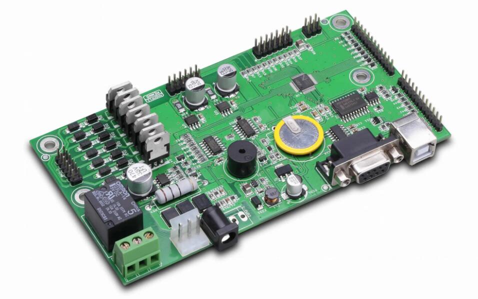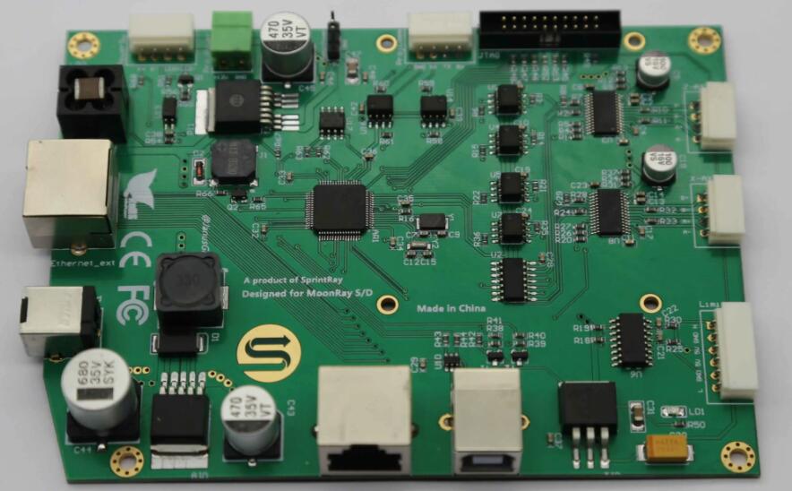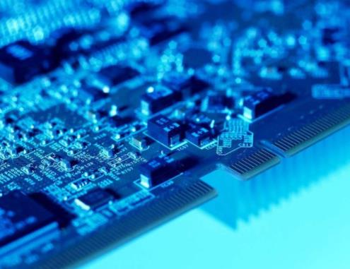

Double-sided PCBs play a crucial role in the design and production of modern electronic products. As electronic devices become increasingly miniaturized and complex, Double Layer PCBs have become the preferred choice for many applications due to their high density and reliability. This article explores the basic principles, advantages, and applications of Double Layer PCBs in real-world production.
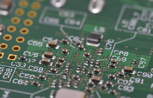
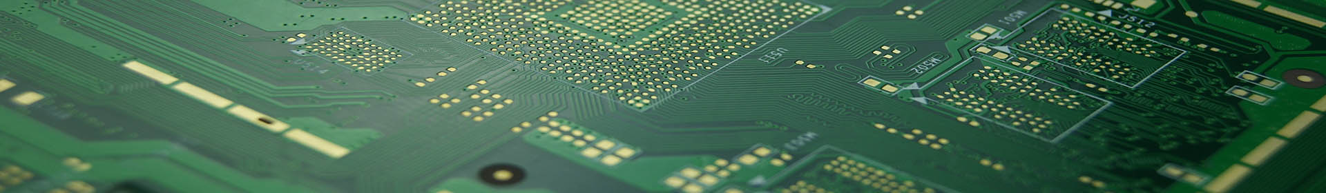
Double-sided PCBis a printed circuit board that allows wiring on both sides. This design enables more circuits and more complex designs to be implemented in a smaller area. Using through-hole technology, Double Layer PCBs can achieve electrical connections between the top and bottom sides, significantly enhancing the design flexibility and functionality of the circuit board.In the production process, the manufacturing steps of a Double Layer PCB include substrate selection, lamination, drilling, copper plating, photolithography, etching, and surface treatment. The first section of the article mentions that the core advantage of a Double Layer PCB is its ability to carry more components and circuits, thereby improving the overall performance and reliability of the circuit.
The first paragraph mentions that one of the advantages of a Double Layer PCB is its ability to utilize space more effectively. Since wiring can be done on both sides, designers can achieve more functionality in a smaller area. This is particularly important for space-constrained devices such as smartphones, tablets, and portable electronics.Double Layer PCB is its high reliability. Through the use of through-hole technology, Double Layer PCBs can achieve more stable electrical connections, reducing failures and enhancing the durability of the equipment. Additionally, Double Layer PCBs can better manage heat, helping to extend the lifespan of components.

Double-sided PCBs
Double-sided PCBs perform excellently. Due to their good conductivity and low signal interference, Double Layer PCBs are widely used in wireless communications, radar systems, and high-frequency sensors. Their high density and reliability make them an ideal choice for these high-performance applications.Although Double Layer PCBs have many advantages, their manufacturing process is relatively complex and costly. Designers and manufacturers need to carefully select materials and processes to ensure the quality and performance of the final product. Additionally, the design of Double Layer PCBs must consider issues such as electromagnetic compatibility (EMC) and thermal management to avoid failures in actual applications.
Moreover, Double Layer PCBs are increasingly used in medical devices. The precision and reliability of these PCBs are critical for devices such as pacemakers, diagnostic equipment, and medical imaging systems. The ability to design compact and reliable circuits on both sides of the PCB allows for the development of smaller, more efficient medical devices, enhancing patient care and treatment outcomes.In the field of industrial automation, Double Layer PCBs are essential for controlling machinery and processes. Their high density allows for the integration of complex control systems in a compact form, improving efficiency and reducing space requirements. This is particularly important in industries where space and reliability are crucial, such as in robotics and factory automation.
The adoption of Double-sided PCBs in consumer electronics is also noteworthy. Devices such as laptops, gaming consoles, and wearable technology rely on the compact and efficient design capabilities of Double Layer PCBs. These PCBs support high-speed data processing and complex functionalities, meeting the demanding requirements of modern consumers.Furthermore, advancements in Double Layer PCB manufacturing techniques, such as automated optical inspection (AOI) and advanced soldering technologies, have improved the production yield and quality of these PCBs. AOI systems can quickly and accurately detect defects, ensuring that only high-quality PCBs proceed to the next stages of production. This reduces the overall cost and improves the reliability of electronic devices.
The environmental impact of Double Layer PCB production is another important consideration. Manufacturers are increasingly adopting eco-friendly practices, such as using lead-free solder and recycling materials, to reduce the environmental footprint of PCB production. These practices not only help in complying with environmental regulations but also contribute to sustainable manufacturing processes.
Double Layer PCBs hold an irreplaceable position in the design and production of modern electronic products. Their high density, high reliability, and good conductivity make them widely used in many fields. In terms of innovation, the integration of flexible circuits with Double Layer PCBs opens up new possibilities for electronic design. Flexible Double Layer PCBs can be bent and shaped to fit into unconventional spaces, providing new design opportunities for wearable technology, flexible displays, and other innovative applications. This flexibility enhances the functionality and aesthetic appeal of electronic products.As technology continues to advance, Double Layer PCBs will continue to drive innovation and development in electronic products.