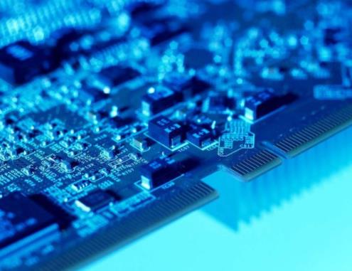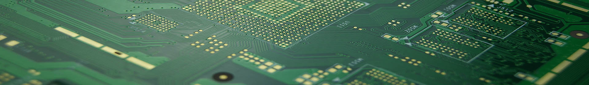

Laser annealing semiconductor technology has seen widespread adoption in recent years, particularly in the field of printed circuit board (PCB) design and production. Laser annealing, a process that involves heating materials with a laser beam to alter their physical and chemical properties, holds a significant position in semiconductor manufacturing. This article will explore the applications and advantages of Laser treatment of semiconductors technology in PCB design and production.
Laser annealing semiconductor technology is increasingly being applied in PCB design. Traditional annealing methods usually require prolonged high-temperature treatment, whereas laser annealing can complete the annealing process in an extremely short period. This not only significantly improves production efficiency but also reduces the heat-affected zones, thereby enhancing the performance and reliability of the product. In PCB design, laser annealing can help optimize the electrical conductivity of circuits, reduce resistance, and improve the overall efficiency of the circuit.
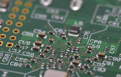
During the production process, Laser treatment of semiconductors technology can greatly enhance manufacturing precision and quality. Due to the high precision and controllability of the laser beam, the annealing process can be very accurately localized to the areas that need treatment, avoiding unnecessary thermal damage. Additionally, laser annealing can improve the crystalline structure of materials, enhancing their electrical properties and mechanical strength. This is particularly important for manufacturing high-performance and highly reliable PCBs.

Laser annealing semiconductor
Laser annealing semiconductor technology offers unique advantages in the production of miniaturized and high-density PCBs. As electronic devices continue to miniaturize, PCB designs are becoming more complex and compact. Laser annealing technology can precisely process very small areas, meeting the manufacturing needs of high-density wiring and tiny components. By optimizing the annealing process, micro-defects can be effectively reduced, enhancing the stability and reliability of the circuit.Looking ahead, Laser treatment of semiconductors technology is expected to play a crucial role in more fields. With continuous technological advancements, the application scope of laser annealing will further expand beyond PCB design and production to include other high-tech fields such as semiconductor chip manufacturing, optoelectronic devices, and new energy materials. The ongoing innovation in laser annealing technology will bring more possibilities and development opportunities to various industries.
The implementation of Laser treatment of semiconductors technology brings several additional benefits that extend beyond the immediate improvements in PCB manufacturing. One notable advantage is the potential for significant energy savings. Traditional thermal annealing processes require substantial energy input to maintain high temperatures over extended periods. In contrast, laser annealing focuses energy precisely where it is needed, reducing overall energy consumption and making the process more environmentally friendly.
Laser annealing semiconductor technology can contribute to the development of more durable and resilient electronic devices. By precisely controlling the annealing process, manufacturers can achieve better material uniformity and eliminate micro-cracks and other defects that can lead to device failure. This results in electronic components that are more robust and capable of withstanding demanding operational conditions, thereby extending the lifespan of the final products.Another area where Laser treatment of semiconductors technology shows promise is in the enhancement of flexible and wearable electronics. These types of devices require highly flexible and reliable circuit boards that can endure bending and stretching without performance degradation. Laser annealing can enhance the mechanical properties of the materials used in these applications, ensuring that the electronic components maintain their functionality even under significant physical stress.
Additionally, the precision of Laser treatment of semiconductors technology makes it ideal for producing advanced semiconductor devices with complex architectures. As semiconductor devices become more intricate, with smaller and more densely packed features, the need for precise and localized thermal processing becomes critical. Laser annealing can achieve the necessary precision, enabling the production of next-generation semiconductor devices that are faster, more efficient, and more powerful.
laser annealing semiconductor technology, as an advanced manufacturing process, is continuously driving progress in PCB design and production. By enhancing manufacturing precision, optimizing electrical performance, and improving material quality, this technology not only meets the high standards of current electronic products but also lays a solid foundation for future technological innovations.