

This article will introduce the standard 4 layer pcb stackup in detail, its structure, design points, manufacturing process and its application scenarios, providing a comprehensive reference for engineers and designers.
Printed circuit boards (PCBs) are a core component of modern electronic equipment. In complex electronic devices, multi-layer PCBs are widely used, among which 4-layer PCBs have become one of the most common choices due to their balanced performance and cost advantages.
1. Standard 4 layer pcb stackup structure
1.1 Standard stacked structure (from top to bottom):
Top Layer: used for placing components and wiring.
Inner Layer 1: As the ground layer (GND), it is used to provide electromagnetic shielding and signal reference.
Inner Layer 2: As the power layer (Power), used for power distribution.
Bottom Layer: used for placing components and wiring.
This stacked structure provides good electrical performance and signal integrity and is suitable for most moderately complex electronic designs.
1.2 Interlayer dielectric material
The dielectric material between layers is usually pre-impregnated fiberglass cloth (Prepreg) or core board (Core). The dielectric constant and thickness of these materials directly affect the impedance control and signal integrity of the PCB.
1.3 Routing and spacing
When designing a 4-layer PCB, trace width and spacing need to be considered. Typically, signal layers have trace widths and spacing of 0.1-0.2 mm, while power and ground layers are designed based on current requirements.

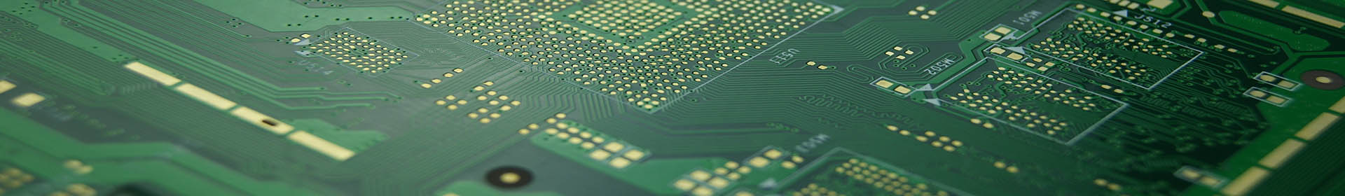
Standard 4 layer pcb stackup
2. Standard 4 layer pcb stackupdesign points
2.1 Power and ground layering
Power and ground layering is at the heart of multilayer PCB design. Using inner layer 1 as the ground layer and inner layer 2 as the power layer can effectively reduce the noise between the power supply and ground and provide stable power distribution.
2.2 Signal integrity
In multi-layer PCBs, signal integrity is key to the design. The top and bottom layers are typically used for high-speed signal routing, while the inner layers are used for low-speed signal and power distribution. Through reasonable wiring and inter-layer via design, signal reflection and crosstalk can be effectively reduced.
2.3 Impedance control
In order to ensure the stability of signal transmission, precise impedance control is necessary. By selecting appropriate dielectric materials and controlling trace width and spacing, a differential impedance of 50 ohms or 100 ohms can be achieved.
3. Standard 4 layer pcb stackup manufacturing process
3.1 Material selection
Choosing high-quality substrates and pre-impregnated fiberglass cloth is the basis for ensuring PCB performance. Commonly used materials include FR4, Rogers, etc., with different dielectric constants and thermal expansion coefficients.
3.2 Laminated lamination
Laminated lamination is a key process in multi-layer PCB manufacturing. Each layer of material is pressed together under high temperature and high pressure by a hot press to form a strong multi-layer structure.
3.3 Plating and etching
After lamination is completed, circuit patterns are formed through electroplating and etching processes. The electroplated copper layer provides good electrical conductivity and mechanical strength, while the etching process removes excess copper layer to form fine circuit patterns.
3.4 Surface treatment
Surface treatment processes include hot air leveling (HASL), electroless nickel gold plating (ENIG), etc., providing good weldability and oxidation resistance.
4. Application scenarios
4.1 Consumer electronics
In consumer electronics such as smartphones and tablets, 4-layer PCBs are widely used due to their high performance and low cost. Its multi-layer construction provides excellent electromagnetic compatibility and signal integrity.
4.2 Communication equipment
In communication equipment such as routers and switches, 4-layer PCB can support high-speed signal transmission and complex power management requirements to ensure stable operation of the equipment.
4.3 Industrial control
In industrial automation and control systems, 4-layer PCBs can meet the requirements for high reliability and durability. Its multi-layer structure provides sufficient power and signal distribution capabilities to adapt to complex industrial environments.
4.4 Automotive electronics
In automotive electronic systems, such as central control displays, in-car entertainment, etc., 4-layer PCB provides high immunity and stable power distribution to ensure reliable operation of the system.
Standard 4 layer pcb stackup has become an important choice in modern electronic design due to its superior performance and economy. Through reasonable lamination design and manufacturing process, high reliability and high performance circuit boards can be achieved to meet the needs of various complex applications. We hope this guide can help engineers and designers better understand and apply 4-layer PCB technology and promote the development of the electronics industry.


